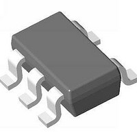
AAT4900IGV-T1 Analogic Tech, AAT4900IGV-T1 Datasheet

AAT4900IGV-T1
Specifications of AAT4900IGV-T1
Available stocks
Related parts for AAT4900IGV-T1
AAT4900IGV-T1 Summary of contents
Page 1
General Description The AAT4900 FastSwitch is a member of AnalogicTech's Application MOSFET™ (ASPM™) product family. buffered power half-bridge, consisting of low on resistance power MOSFETs with integrated control logic. This device operates with inputs ranging from 2.0V to 5.5V, making ...
Page 2
Pin Descriptions Pin # SOT23-5 SC70JW Pin Configuration SOT23-5 (Top View GND Control Logic Table CLK Symbol ...
Page 3
Absolute Maximum Ratings T = 25°C, unless otherwise noted. A Symbol Description GND EN, CLK to GND EN CLK V OUT to GND OUT I Maximum Continuous Switch Current MAX T Operating Junction ...
Page 4
Electrical Characteristics -40°C to +85°C, unless otherwise noted. Typical values are Symbol Description V Operation Voltage Quiescent Current QAC I DC Quiescent Current QDC I Off-Supply Current Q(OFF) ...
Page 5
Typical Characteristics Operating Current vs. Input Voltage (F = 1MHz 2.5 3.0 3.5 4.0 4.5 Input Voltage (V) Operating Current vs. Temperature (F = 1MHz ...
Page 6
Typical Characteristics High Side R 0. 2.7V, 0. 2.2A D 0.20 0.15 0. 5.5V 0.2A to 2.2A 0.05 D 0.00 -40 - Temperature (°C) Propagation Delay vs. ...
Page 7
Functional Block Diagram CLK EN Typical Applications DC/DC Converter The most common AAT4900 applications include a DC/DC converter output power stage and a MOS- FET gate drive buffer. Figure 1 shows a common configuration when used as a DC/DC converter ...
Page 8
Synchronous Buck DC/DC Converter Application The losses associated with the AAT4900 high side switching MOSFET are due to switching losses and conduction losses. The conduction losses are asso- ciated with the R characteristics of the output DS(ON) switching device. At ...
Page 9
Gate Drive When used as a MOSFET gate driver, the break- before-make shoot-through protection significantly reduces losses associated with the driver at high frequencies. (See Figure 2.) The low R of the output stage allows for a DS(ON) high peak ...
Page 10
Motor Drive The AAT4900 is also ideally suited for use as an effi- cient output driver for DC brushless motor control. The inductive load switching capability of the AAT4900 eliminates the need for external diodes. A typical motor control circuit ...
Page 11
CLK LX Figure 5: Timing Diagram. 50% CLK 50 PLH 90% LX 10% Figure 6: Switching Time Waveforms CLK GND Figure 7: Propagation Delay Test Circuit. AAT4900 Buffered Power Half-Bridge PHL t ...
Page 12
... All dimensions in millimeters. 1. XYY = assembly and date code. 2. Sample stock is generally held on part numbers listed in BOLD. 12 Buffered Power Half-Bridge Marking Part Number (Tape and Reel) 1 ABXYY AAT4900IGV-T1 ABXYY AAT4900IJS-T1 SOT23-5 0.075 ± 0.075 0.60 REF AAT4900 2 0.15 ± 0.07 GAUGE PLANE 0.45 ± ...
Page 13
... AnalogicTech deems necessary to support this warranty. Specific testing of all parameters of each device is not necessarily performed. AnalogicTech and the AnalogicTech logo are trademarks of Advanced Analogic Technologies Incorporated. All other brand and product names appearing in this document are regis- tered trademarks or trademarks of their respective holders ...


