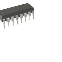
SI9110DJ-E3 Vishay, SI9110DJ-E3 Datasheet - Page 5

SI9110DJ-E3
Manufacturer Part Number
SI9110DJ-E3
Description
Switching Converters, Regulators & Controllers HV Switchmode Cont
Manufacturer
Vishay
Specifications of SI9110DJ-E3
Output Voltage
13.5 V
Output Current
- 2 mA
Operating Temperature Range
- 40 C to + 85 C
Input Voltage
10 V to 120 V
Switching Frequency
40 KHz to 1 MHz
Mounting Style
Through Hole
Duty Cycle (max)
50 %
Package / Case
DIP-14
Number Of Outputs
2
Primary Input Voltage
120V
No. Of Outputs
1
No. Of Pins
14
Peak Reflow Compatible (260 C)
No
Pwm Type
Current Mode PWM Controller
Number Of Pwm Outputs
1
On/off Pin
Yes
Adjustable Output
No
Topology
Flyback/Forward/Push-Pull
Switching Freq
1000kHz
Operating Supply Voltage (max)
13.5V
Synchronous Pin
No
Rise Time
40ns
Fall Time
40ns
Operating Temperature Classification
Industrial
Mounting
Through Hole
Pin Count
14
Package Type
PDIP
Lead Free Status / RoHS Status
Lead free / RoHS Compliant
Lead Free Status / RoHS Status
Lead free / RoHS Compliant, Lead free / RoHS Compliant
DETAILED DESCRIPTION
Pre-Regulator/Start-Up Section
Due to the low quiescent current requirement of the
Si9110/9111 control circuitry, bias power can be supplied from
the unregulated input power source, from an external
regulated low-voltage supply, or from an auxiliary “bootstrap”
winding on the output inductor or transformer.
When power is first applied during start-up, +V
draw a constant current. The magnitude of this current is
determined by a high-voltage depletion MOSFET device
which is connected between +V
start-up circuitry provides initial power to the IC by charging an
external bypass capacitance connected to the V
constant current is disabled when V
not forced to exceed the 8.6-V threshold, then V
regulated to a nominal value of 8.6 V by the pre-regulator
circuit.
As the supply voltage rises toward the normal operating
conditions, an internal undervoltage (UV) lockout circuit keeps
the output driver disabled until V
lockout threshold (typically 8.1 V). This guarantees that the
control logic will be functioning properly and that sufficient
gate drive voltage is available before the MOSFET turns on.
The design of the IC is such that the undervoltage lockout
threshold will be at least 300 mV less than the pre-regulator
turn-off voltage. Power dissipation can be minimized by
providing an external power source to V
constant current source is always disabled.
Note: During start-up or when V
start-up circuit is capable of sourcing up to 20 mA. This may
Document Number: 70004
S-42037—Rev. H, 15-Nov-04
OSC OUT
PIN CONFIGURATIONS AND ORDERING INFORMATION
OUTPUT
SENSE
BIAS
+V
−V
V
CC
IN
IN
Dual-In-Line and SOIC
1
2
3
4
5
6
7
Top View
14
13
12
10
11
9
8
FB
COMP
RESET
SHUTDOWN
V
DISCHARGE
OSC IN
REF
CC
IN
CC
CC
exceeds the undervoltage
and V
exceeds 8.6 V. If V
drops below 8.6 V the
CC
CC
such that the
IN
(pin 6). This
CC
(pin 2) will
CC
pin. The
will be
CC
is
lead to a high level of power dissipation in the IC (for a 48-V
input, approximately 1 W). Excessive start-up time caused by
external loading of the V
damage. Figure 6 gives the typical pre-regulator current at
BiC/DMOS as a function of input voltage.
BIAS
To properly set the bias for the Si9110/9111, a 390-kW resistor
should be tied from BIAS (pin 1) to −V
determines the magnitude of bias current in all of the analog
sections and the pull-up current for the SHUDOWN and
RESET pins. The current flowing in the bias resistor is
nominally 15 mA.
Reference Section
The reference section of the Si9110 consists of a temperature
compensated buried zener and trimmable divider network.
The output of the reference section is connected internally to
the non-inverting input of the error amplifier. Nominal reference
output voltage is 4 V. The trimming procedure that is used on
the Si9110 brings the output of the error amplifier (which is
configured for unity gain during trimming) to within "1% of 4 V.
This compensates for input offset voltage in the error amplifier.
The output impedance of the reference section has been
purposely made high so that a low impedance external voltage
source can be used to override the internal voltage source, if
desired, without otherwise altering the performance of the device.
Si9110DY
Si9110DY-T1
Si9110DY-T1—E3
Si9111DY
Si9111DY-T1
Si9111DY-T1—E3
Si9110DJ
Si9110DJ-—E3
Si9111DJ
Si9111DJ-—E3
Part Number
ORDERING INFORMATION
Temperature Range
−40 to 85_C
−40 to 85_C
CC
supply can result in device
Vishay Siliconix
Si9110/9111
IN
Package
(pin 5). This
www.vishay.com
SOIC-14
SOIC-14
PDIP 14
PDIP-14
5


