AGLN015V2-QNG68 Actel, AGLN015V2-QNG68 Datasheet - Page 18
AGLN015V2-QNG68
Manufacturer Part Number
AGLN015V2-QNG68
Description
FPGA - Field Programmable Gate Array 15K System Gates IGLOO nano
Manufacturer
Actel
Datasheet
1.AGLN030V5-ZUCG81.pdf
(140 pages)
Specifications of AGLN015V2-QNG68
Processor Series
AGLN015
Core
IP Core
Number Of Macrocells
128
Maximum Operating Frequency
250 MHz
Number Of Programmable I/os
49
Supply Voltage (max)
1.5 V
Supply Current
6 uA
Maximum Operating Temperature
+ 70 C
Minimum Operating Temperature
- 20 C
Development Tools By Supplier
AGLN-Nano-Kit, AGLN-Z-Nano-Kit, AGL-Dev-Kit-SCS, Silicon-Explorer II, Silicon-Sculptor 3, SI-EX-TCA, FLASHPRO 4, FlashPro 3, FLASHPRO LITE
Mounting Style
SMD/SMT
Supply Voltage (min)
1.2 V
Number Of Gates
15 K
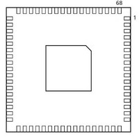
Package / Case
QFN-68
Lead Free Status / RoHS Status
Lead free / RoHS Compliant


IGLOO nano DC and Switching Characteristics
Figure 2-1 • V5 Devices – I/O State as a Function of VCCI and VCC Voltage Levels
2- 4
Deactivation trip point:
Activation trip point:
V
V
a
d
= 0.85 V ± 0.25 V
= 0.75 V ± 0.25 V
VCC = 1.575 V
VCC = 1.425 V
PLL Behavior at Brownout Condition
Actel recommends using monotonic power supplies or voltage regulators to ensure proper power-up
behavior. Power ramp-up should be monotonic at least until VCC and VCCPLX exceed brownout
activation levels (see
When PLL power supply voltage and/or VCC levels drop below the VCC brownout levels (0.75 V ± 0.25
V for V5 devices, and 0.75 V ± 0.2 V for V2 devices), the PLL output lock signal goes LOW and/or the
output clock is lost. Refer to the "Brownout Voltage" section in the "Power-Up/-Down Behavior of Low
Power Flash Devices" chapter of the
and lock recovery.
Internal Power-Up Activation Sequence
To make sure the transition from input buffers to output buffers is clean, ensure that there is no path
longer than 100 ns from input buffer to output buffer in your design.
VCC
1. Core
2. Input buffers
3. Output buffers, after 200 ns delay from input buffer activation
Region 1: I/O Buffers are OFF
VCC = VCCI + VT
where VT can be from 0.58 V to 0.9 V (typically 0.75 V)
Deactivation trip point:
Activation trip point:
V
V
d
a
= 0.9 V ± 0.3 V
= 0.8 V ± 0.3 V
Figure 2-1
Region 1: I/O buffers are OFF
Region 2: I/O buffers are ON.
I/Os are functional but slower because
VCCI / VCC are below specification. For the
same reason, input buffers do not meet
VIH/VIL levels, and output buffers to not
meet VOH / VOL levels.
buffers do not meet VOH/VOL levels.
and
meet VIH / VIL levels, and output
same reason, input buffers do not
Figure 2-2 on page 2-5
is below specification. For the
IGLOO nano FPGA Fabric User’s Guide
but slower because VCCI
R ev isio n 1 1
I/Os are functional
buffers are ON.
Region 4: I/O
Min VCCI datasheet specification
standard; i.e., 1.425 V or 1.7 V
voltage at a selected I/O
or 2.3 V or 3.0 V
for more details).
Region 3: I/O buffers are ON.
I/Os are functional; I/O DC
specifications are met,
but I/Os are slower because
the VCC is below specification.
Region 5: I/O buffers are ON
and power supplies are within
specification.
I/Os meet the entire datasheet
and timer specifications for
speed, VIH / VIL , VOH / VOL , etc.
for information on clock
V
CCI
Related parts for AGLN015V2-QNG68
Image
Part Number
Description
Manufacturer
Datasheet
Request
R

Part Number:
Description:
AGLN015V2-QNG68I
Manufacturer:
Actel
Datasheet:
Part Number:
Description:
MCU, MPU & DSP Development Tools Silicon Sculptor Programming Mod
Manufacturer:
Actel
Part Number:
Description:
MCU, MPU & DSP Development Tools InSystem Programming ProASICPLUS Devices
Manufacturer:
Actel
Part Number:
Description:
Programming Socket Adapters & Emulators PQ160 Module
Manufacturer:
Actel
Part Number:
Description:
Programming Socket Adapters & Emulators Axcelerator Adap Module Kit
Manufacturer:
Actel
Part Number:
Description:
Programming Socket Adapters & Emulators Evaluation
Manufacturer:
Actel
Part Number:
Description:
Programming Socket Adapters & Emulators AFDX Solutions
Manufacturer:
Actel
Part Number:
Description:
Programming Socket Adapters & Emulators SILICON SCULPTOR ADAPTER MODULE
Manufacturer:
Actel
Datasheet:
Part Number:
Description:
Programming Socket Adapters & Emulators Axcelerator Adap Module Kit
Manufacturer:
Actel
Part Number:
Description:
Programming Socket Adapters & Emulators Evaluation
Manufacturer:
Actel
Part Number:
Description:
Programming Socket Adapters & Emulators Silicon Sculptor Software
Manufacturer:
Actel
Part Number:
Description:
Programming Socket Adapters & Emulators InSystem Programming ProASICPLUS Devices
Manufacturer:
Actel
Part Number:
Description:
Programming Socket Adapters & Emulators Evaluation
Manufacturer:
Actel
Part Number:
Description:
Programming Socket Adapters & Emulators Axcelerator Adap Module Kit
Manufacturer:
Actel
Part Number:
Description:
Programming Socket Adapters & Emulators Axcelerator Adap Module Kit
Manufacturer:
Actel