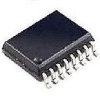
DG442DY-E3 Vishay, DG442DY-E3 Datasheet - Page 8

DG442DY-E3
Manufacturer Part Number
DG442DY-E3
Description
Analog Switch ICs SPST Analog Switch
Manufacturer
Vishay
Type
Analog Switchr
Datasheet
1.DG441DY-T1-E3.pdf
(9 pages)
Specifications of DG442DY-E3
Number Of Switches
Quad
Switch Configuration
SPST
On Resistance (max)
160 Ohms
On Time (max)
450 ns
Off Time (max)
200 ns
Supply Voltage (max)
25 V
Supply Current
0.015 mA
Maximum Power Dissipation
900 mW
Maximum Operating Temperature
+ 85 C
Mounting Style
SMD/SMT
Package / Case
SOIC-16 Narrow
Minimum Operating Temperature
- 40 C
Analog Switch Type
SPST
No. Of Channels
4
On State Resistance Max
85ohm
Turn Off Time
110ns
Turn On Time
150ns
Supply Voltage Range
10.8V To 13.2V
Multiplexer Configuration
Quad SPST
Number Of Inputs
4
Number Of Outputs
4
Number Of Channels
4
Analog Switch On Resistance
160@10.8VOhm
Power Supply Requirement
Single/Dual
Single Supply Voltage (min)
13V
Single Supply Voltage (typ)
15/18/24/28V
Single Supply Voltage (max)
36V
Dual Supply Voltage (min)
±7V
Dual Supply Voltage (typ)
±9/±12/±15/±18V
Dual Supply Voltage (max)
±22V
Power Dissipation
900mW
Mounting
Surface Mount
Pin Count
16
Operating Temp Range
-40C to 85C
Operating Temperature Classification
Industrial
Package
16SOIC N
Maximum On Resistance
160@10.8V Ohm
Maximum High Level Output Current
30 mA
Maximum Turn-off Time
210@±15V ns
Maximum Turn-on Time
450@12V ns
Switch Architecture
SPST
Power Supply Type
Single|Dual
Lead Free Status / RoHS Status
Lead free / RoHS Compliant
Lead Free Status / RoHS Status
Lead free / RoHS Compliant, Lead free / RoHS Compliant
DG441/442
Vishay Siliconix
APPLICATIONS
Vishay Siliconix maintains worldwide manufacturing capability. Products may be manufactured at one of several qualified locations. Reliability data for Silicon
Technology and Package Reliability represent a composite of all qualified locations. For related documents such as package/tape drawings, part marking, and
reliability data, see http://www.vishay.com/ppg?70053.
www.vishay.com
8
+ 15 V
IN
0 = Load Off
1 = Load On
Figure 7. Power MOSFET Driver
DG442
GND
GAIN
A
GAIN
A
GAIN
A
GAIN
A
V
V
V
V
= 100
= 1
= 10
= 20
4
1
2
3
+ 15 V
V
V+
IN
V-
Figure 9. Precision-Weighted Resistor Programmable-Gain Amplifier
150
10
- 15 V
kΩ
DG441 or DG442
V+
V-
Ω
+ 15 V
+
-
+ 15 V
VN0300 L, M
+ 24 V
GND
R
I = 3 A
L
R
90
R
5
R
4
R
1
1
2
3
4
kΩ
kΩ
kΩ
kΩ
V
IN
IN
Gain error is determined only by the resistor
tolerance. Op amp offset and CMRR will limit ac-
curacy of circuit.
With SW
V
+
-
V
OUT
IN
Figure 8. Open Loop Sample-and-Hold
4
=
V
Closed
OUT
S
R
1/4 DG442
1
+ R
2
R
+ R
+ 15 V
4
- 15 V
3
D
+ R
4
S-71241–Rev. I, 25-Jun-07
Document Number: 70053
H = Sample
L = Hold
= 100
C
H
+
-
V
OUT


