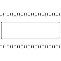
MAX4936CTN+ Maxim Integrated Products, MAX4936CTN+ Datasheet - Page 10

MAX4936CTN+
Manufacturer Part Number
MAX4936CTN+
Description
Multiplexer Switch ICs OCTAL HV T/R SWITCH Octal HV T/R Switch
Manufacturer
Maxim Integrated Products
Datasheet
1.MAX4936CTN.pdf
(19 pages)
Specifications of MAX4936CTN+
Number Of Channels
8 Channel
On Time (max)
200 ns
Off Time (max)
100 ns
Supply Voltage (max)
5.5 V
Supply Voltage (min)
1.62 V
Supply Current
1.5 mA
Maximum Power Dissipation
3279 mW
Maximum Operating Temperature
+ 70 C
Minimum Operating Temperature
0 C
Package / Case
TQFN-56
Mounting Style
SMD/SMT
Off Isolation (typ)
- 50 dB
Off State Leakage Current (max)
3 uA
Lead Free Status / RoHS Status
Lead free / RoHS Compliant
Octal High-Voltage Transmit/Receive Switches
10
3, 6, 15, 18, 54
MAX4936/
12, 23, 53
MAX4938
_____________________________________________________________________________________
10
11
13
14
16
17
19
20
21
22
4
5
7
8
9
PIN
13, 15, 16, 18,
19, 21, 54, 56
2, 3, 5, 6, 8,
MAX4937/
MAX4939
12, 23, 53
10
11
14
17
20
22
—
—
—
—
—
—
4
7
9
NAME
COM3
COM4
COM5
COM6
COM7
COM8
GND
N.C.
HV3
HV4
V
V
HV5
HV6
HV7
HV8
V
DD
CC
EE
No Connection. Not internally connected.
T/R Switch 3 Input. When the switch is on, low-voltage signals are passed
through from COM3 to NO3, while high-voltage signals are blocked. When the
switch is off, both low-voltage and high-voltage signals are blocked.
T/R Switch 3 Input. COM3 follows HV3 when high-voltage signals are present on
HV3. HV3 is isolated from COM3 when low-voltage signals are present on COM3.
T/R Switch 4 Input. When the switch is on, low-voltage signals are passed
through from COM4 to NO4, while high-voltage signals are blocked. When the
switch is off, both low-voltage and high-voltage signals are blocked.
T/R Switch 4 Input. COM4 follows HV4 when high-voltage signals are present on
HV4. HV4 is isolated from COM4 when low-voltage signals are present on COM4.
Positive Logic Supply. Bypass V
capacitor as close as possible to the device.
Positive Analog Supply. Bypass V
capacitor as close as possible to the device.
Negative Analog Supply. Bypass V
capacitor as close as possible to the device.
Ground
T/R Switch 5 Input. COM5 follows HV5 when high-voltage signals are present on
HV5. HV5 is isolated from COM5 when low-voltage signals are present on COM5.
T/R Switch 5 Input. When the switch is on, low-voltage signals are passed
through from COM5 to NO5, while high-voltage signals are blocked. When the
switch is off, both low-voltage and high-voltage signals are blocked.
T/R Switch 6 Input. COM6 follows HV6 when high-voltage signals are present on
HV6. HV6 is isolated from COM6 when low-voltage signals are present on COM6.
T/R Switch 6 Input. When the switch is on, low-voltage signals are passed
through from COM6 to NO6, while high-voltage signals are blocked. When the
switch is off, both low-voltage and high-voltage signals are blocked.
T/R Switch 7 Input. COM7 follows HV7 when high-voltage signals are present on
HV7. HV7 is isolated from COM7 when low-voltage signals are present on COM7.
T/R Switch 7 Input. When the switch is on, low-voltage signals are passed
through from COM7 to NO7, while high-voltage signals are blocked. When the
switch is off, both low-voltage and high-voltage signals are blocked.
T/R Switch 8 Input. COM8 follows HV8 when high-voltage signals are present on
HV8. HV8 is isolated from COM8 when low-voltage signals are present on COM8.
T/R Switch 8 Input. When the switch is on, low-voltage signals are passed
through from COM8 to NO8, while high-voltage signals are blocked. When the
switch is off, both low-voltage and high-voltage signals are blocked.
DD
Pin Description (continued)
CC
FUNCTION
EE
to GND with a 1FF or greater ceramic
to GND with a 1FF or greater ceramic
to GND with a 1FF or greater ceramic


