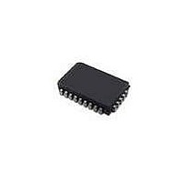
DG406DN-E3 Vishay, DG406DN-E3 Datasheet - Page 8

DG406DN-E3
Manufacturer Part Number
DG406DN-E3
Description
Multiplexer Switch ICs Single 16:1, 4-bit Multiplexer/MUX
Manufacturer
Vishay
Type
Analog Multiplexerr
Datasheet
1.DG406DN-T1-E3.pdf
(11 pages)
Specifications of DG406DN-E3
Supply Current
0.05 mA
On Resistance (max)
120 Ohms
Propagation Delay Time
350 ns
On Time (max)
600 ns
Off Time (max)
300 ns
Supply Voltage (max)
25 V
Maximum Power Dissipation
450 mW
Maximum Operating Temperature
+ 85 C
Minimum Operating Temperature
- 40 C
Package / Case
PLCC-28
Mounting Style
SMD/SMT
Number Of Switches
Single
No. Of Circuits
1
On State Resistance Max
50ohm
Supply Voltage Range
± 5V To ± 20V
Operating Temperature Range
-40°C To +85°C
Analog Switch Case Style
LCC
Multiplexer Configuration
Single 16:1
Number Of Inputs
16
Number Of Outputs
1
Number Of Channels
1
Analog Switch On Resistance
120@12VOhm
Package Type
PLCC
Power Supply Requirement
Single/Dual
Single Supply Voltage (typ)
9/12/15/18/24/28V
Single Supply Voltage (max)
44V
Dual Supply Voltage (min)
±5V
Dual Supply Voltage (typ)
±9/±12/±15/±18V
Dual Supply Voltage (max)
±20V
Power Dissipation
450mW
Mounting
Surface Mount
Pin Count
28
Operating Temp Range
-40C to 85C
Operating Temperature Classification
Industrial
Package
28PLCC
Maximum On Resistance
120@12V Ohm
Maximum Propagation Delay Bus To Bus
350@±15V ns
Maximum High Level Output Current
30 mA
Multiplexer Architecture
16:1
Maximum Turn-off Time
300@12V ns
Maximum Turn-on Time
600@12V ns
Power Supply Type
Single|Dual
Lead Free Status / RoHS Status
Lead free / RoHS Compliant
Lead Free Status / RoHS Status
Lead free / RoHS Compliant, Lead free / RoHS Compliant
Available stocks
Company
Part Number
Manufacturer
Quantity
Price
DG406, DG407
Vishay Siliconix
SCHEMATIC DIAGRAM (Typical Channel)
TEST CIRCUITS
www.vishay.com
8
+ 2.4 V
+ 2.4 V
GND
EN
V+
A
V-
A
X
0
50
50
* = S
Ω
Ω
EN
1a
EN
A
A
A
A
A
A
A
3
2
1
0
2
1
0
- S
V
GND
GND
REF
8a
DG406
DG407
, S
V+
V+
2b
V+
- 15 V
- 15 V
S
+ 15 V
+ 15 V
V-
V-
2
S ±
- S
S
7b
S
S
S
15
16
300
D
, D
300
D
1b
8b
1
*
b
a
Ω
Ω
± 10 V
± 10 V
± 10 V
± 10 V
35 pF
35 pF
Figure 2. Transition Time
Level
Shift
V
V
O
O
Figure 1.
Decode/
Drive
Switch
Output
Logic
V
Input
O
3 V
V
V
0 V
0 V
S1
S8
t
TRA N S
S
1
ON
50 %
S
90 %
8
ON
S11-0179-Rev. J, 07-Feb-11
V+
Document Number: 70061
V-
t
t
r
f
90 %
< 20 ns
< 20 ns
t
TRA N S
D
S
S
1
n


