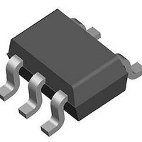
NCP4588DSQ10T1G ON Semiconductor, NCP4588DSQ10T1G Datasheet - Page 2

NCP4588DSQ10T1G
Manufacturer Part Number
NCP4588DSQ10T1G
Description
Low Dropout (LDO) Regulators 200 MA, CAP LESS LV LDO
Manufacturer
ON Semiconductor
Datasheet
1.NCP4588DSQ10T1G.pdf
(17 pages)
Specifications of NCP4588DSQ10T1G
Input Voltage Max
5.25 V
Output Voltage
4.2 V
Dropout Voltage (max)
270 mV
Output Current
400 mA
Load Regulation
25 mV
Voltage Regulation Accuracy
1 %
Maximum Power Dissipation
380 mW
Mounting Style
SMD/SMT
Package / Case
SC-70
Primary Input Voltage
5.25V
Output Voltage Fixed
1V
Dropout Voltage Vdo
640mV
No. Of Pins
5
Voltage Regulator Case Style
SC-70
Operating Temperature Range
-40°C To +85°C
Rohs Compliant
Yes
Lead Free Status / RoHS Status
Lead free / RoHS Compliant
Available stocks
Company
Part Number
Manufacturer
Quantity
Price
Company:
Part Number:
NCP4588DSQ10T1G
Manufacturer:
ON
Quantity:
3 000
Company:
Part Number:
NCP4588DSQ10T1G
Manufacturer:
ON Semiconductor
Quantity:
1 700
Stresses exceeding Maximum Ratings may damage the device. Maximum Ratings are stress ratings only. Functional operation above the
Recommended Operating Conditions is not implied. Extended exposure to stresses above the Recommended Operating Conditions may affect
device reliability.
1. Refer to ELECTRICAL CHARACTERISTIS and APPLICATION INFORMATION for Safe Operating Area.
2. This device series incorporates ESD protection and is tested by the following methods:
VIN
PIN FUNCTION DESCRIPTION
ABSOLUTE MAXIMUM RATINGS
CE
Input Voltage (Note 1)
Output Voltage
Chip Enable Input
Output Current
Power Dissipation XDFN
Power Dissipation SC70
Power Dissipation SOT23
Junction Temperature
Storage Temperature
ESD Capability, Human Body Model (Note 2)
ESD Capability, Machine Model (Note 2)
Pin No.
ESD Human Body Model tested per AEC−Q100−002 (EIA/JESD22−A114)
ESD Machine Model tested per AEC−Q100−003 (EIA/JESD22−A115)
Latchup Current Maximum Rating tested per JEDEC standard: JESD78.
XDFN
4
2
3
6
5
Pin No.
Vref
SC−70
5
3
1
4
2
NCP4588Hxxxxxxx
Current Limit
Pin No.
SOT23
1
2
3
5
4
Rating
Figure 2. Simplified Schematic Block Diagram
Pin Name
VOUT
GND
VIN
NC
CE
VOUT
http://onsemi.com
GND
Input pin
Ground
Chip enable pin (Active “H”)
Output pin
No connection
2
VIN
CE
Symbol
ESD
ESD
Vref
V
I
T
V
OUT
V
P
OUT
T
STG
CE
IN
D
J
HBM
MM
Description
Current Limit
NCP4588Dxxxxxxx
−0.3 to V
−0.3 to 6.0
−40 to 150
−55 to 125
Value
2000
400
400
380
420
200
6.0
IN
+ 0.3
Unit
VOUT
mW
mA
GND
°C
°C
V
V
V
V
V


