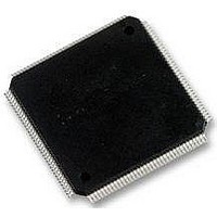
STM32F103ZFT6 STMicroelectronics, STM32F103ZFT6 Datasheet - Page 107

STM32F103ZFT6
Manufacturer Part Number
STM32F103ZFT6
Description
MCU ARM 32BIT 769KB FLSH 144LQFP
Manufacturer
STMicroelectronics
Series
STM32r
Datasheet
1.STM32F103VGT6.pdf
(120 pages)
Specifications of STM32F103ZFT6
Core Processor
ARM® Cortex-M3™
Core Size
32-Bit
Speed
72MHz
Connectivity
CAN, I²C, IrDA, LIN, SPI, UART/USART, USB
Peripherals
DMA, Motor Control PWM, PDR, POR, PVD, PWM, Temp Sensor, WDT
Number Of I /o
112
Program Memory Size
768KB (768K x 8)
Program Memory Type
FLASH
Ram Size
96K x 8
Voltage - Supply (vcc/vdd)
2 V ~ 3.6 V
Data Converters
A/D 21x12b; D/A 2x12b
Oscillator Type
Internal
Operating Temperature
-40°C ~ 85°C
Package / Case
144-LFQFP
Processor Series
STM32F101xF
Core
ARM Cortex M3
Data Bus Width
32 bit
Data Ram Size
80 KB
Interface Type
I2C, SPI, UART
Maximum Clock Frequency
36 MHz
Number Of Programmable I/os
112
Number Of Timers
15
Operating Supply Voltage
2 V to 3.6 V
Maximum Operating Temperature
+ 85 C
Mounting Style
SMD/SMT
Operating Temperature Range
- 40 C to + 105 C
Processor To Be Evaluated
STM32F103ZF
Supply Current (max)
28 mA
Lead Free Status / RoHS Status
Lead free / RoHS Compliant
Eeprom Size
-
Lead Free Status / Rohs Status
Details
Available stocks
Company
Part Number
Manufacturer
Quantity
Price
Company:
Part Number:
STM32F103ZFT6
Manufacturer:
STMicroelectronics
Quantity:
135
Company:
Part Number:
STM32F103ZFT6
Manufacturer:
STMicroelectronics
Quantity:
100
Company:
Part Number:
STM32F103ZFT6
Manufacturer:
STMicroelectronics
Quantity:
10 000
STM32F103xF, STM32F103xG
5.3.20
Table 63.
V
V
V
R
R
C
DAC_OUT
min
DAC_OUT
max
DAC_OUT
min
DAC_OUT
max
I
I
DNL
DDVREF+
DDA
DDA
REF+
SSA
O
LOAD
LOAD
Symbol
(1)
(1)
(1)
(1)
(1)
(2)
(1)
(1)
Analog supply voltage
Reference supply voltage
Ground
Resistive load vs. V
buffer ON
Resistive load vs. V
buffer ON
Impedance output with buffer
OFF
Capacitive load
Lower DAC_OUT voltage
with buffer ON
Higher DAC_OUT voltage
with buffer ON
Lower DAC_OUT voltage
with buffer OFF
Higher DAC_OUT voltage
with buffer OFF
DAC DC current
consumption in quiescent
mode (Standby mode)
DAC DC current
consumption in quiescent
mode (Standby mode)
Differential non linearity
Difference between two
consecutive code-1LSB)
DAC electrical specifications
DAC characteristics
Parameter
SSA
DDA
with
with
2.4
2.4
0
5
15
0.2
Min
Doc ID 16554 Rev 2
0.5
Typ
3.6
3.6
0
15
50
V
V
10 mV
380
380
480
±0.5
±3
DDA
REF+
Max
– 0.2
–
V
V
V
k
k
k
pF
V
V
mV
V
µA
µA
µA
LSB
LSB
Unit
V
When the buffer is OFF, the Minimum
resistive load between DAC_OUT
and V
1.5 M
Maximum capacitive load at
DAC_OUT pin (when the buffer is
ON).
It gives the maximum output
excursion of the DAC.
It corresponds to 12-bit input code
(0x0E0) to (0xF1C) at V
and (0x155) and (0xEAB) at V
2.4 V
It gives the maximum output
excursion of the DAC.
With no load, worst code (0x0E4) at
V
consumption on the inputs
With no load, middle code (0x800) on
the inputs
With no load, worst code (0xF1C) at
V
consumption on the inputs
Given for the DAC in 10-bit
configuration
Given for the DAC in 12-bit
configuration
REF+
REF+
REF+
SS
must always be below V
= 3.6 V in terms of DC
= 3.6 V in terms of DC
Electrical characteristics
to have a 1% accuracy is
Comments
REF+
= 3.6 V
107/120
REF+
DDA
=


