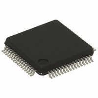
STM32F103RGT6 STMicroelectronics, STM32F103RGT6 Datasheet - Page 94

STM32F103RGT6
Manufacturer Part Number
STM32F103RGT6
Description
MCU ARM 32BIT 1MB FLASH 64LQFP
Manufacturer
STMicroelectronics
Series
STM32r
Datasheet
1.STM32F103VGT6.pdf
(120 pages)
Specifications of STM32F103RGT6
Core Processor
ARM® Cortex-M3™
Core Size
32-Bit
Speed
72MHz
Connectivity
CAN, I²C, IrDA, LIN, SPI, UART/USART, USB
Peripherals
DMA, Motor Control PWM, PDR, POR, PVD, PWM, Temp Sensor, WDT
Number Of I /o
51
Program Memory Size
1MB (1M x 8)
Program Memory Type
FLASH
Ram Size
96K x 8
Voltage - Supply (vcc/vdd)
2 V ~ 3.6 V
Data Converters
A/D 16x12b; D/A 2x12b
Oscillator Type
Internal
Operating Temperature
-40°C ~ 85°C
Package / Case
64-LFQFP
Processor Series
STM32F101xG
Core
ARM Cortex M3
Data Bus Width
32 bit
Data Ram Size
80 KB
Interface Type
I2C, SPI, UART
Maximum Clock Frequency
36 MHz
Number Of Programmable I/os
112
Number Of Timers
15
Operating Supply Voltage
2 V to 3.6 V
Maximum Operating Temperature
+ 85 C
Mounting Style
SMD/SMT
Operating Temperature Range
- 40 C to + 105 C
Processor To Be Evaluated
STM32F103RG
Supply Current (max)
28 mA
Lead Free Status / RoHS Status
Lead free / RoHS Compliant
Eeprom Size
-
Lead Free Status / Rohs Status
Details
Available stocks
Company
Part Number
Manufacturer
Quantity
Price
Company:
Part Number:
STM32F103RGT6
Manufacturer:
STMicroelectronics
Quantity:
135
Company:
Part Number:
STM32F103RGT6
Manufacturer:
STMicroelectronics
Quantity:
10 000
Electrical characteristics
94/120
I
Unless otherwise specified, the parameters given in
are derived from tests performed under ambient temperature, f
supply voltage conditions summarized in
Refer to
function characteristics (NSS, SCK, MOSI, MISO for SPI and WS, CK, SD for I
Table 53.
1. Based on characterization, not tested in production.
2. Min time is for the minimum time to drive the output and the max time is for the maximum time to validate
3. Min time is for the minimum time to invalidate the output and the max time is for the maximum time to put
2
DuCy(SCK)
S - SPI characteristics
t
t
t
t
dis(SO)
t
w(SCKH)
t
w(SCKL)
su(NSS)
t
a(SO)
Symbol
1/t
t
t
t
the data.
the data in Hi-Z
t
t
h(NSS)
t
su(MI)
t
v(SO)
v(MO)
h(MO)
su(SI)
h(MI)
h(SO)
t
t
h(SI)
r(SCK)
f(SCK)
f
c(SCK)
SCK
(1)(2)
(1)
(1)(3)
(1)
(1)
(1)
(1)
(1)
Section 5.3.14: I/O port characteristics
(1)
(1)
(1)
(1)
(1)
(1)
SPI characteristics
SPI clock frequency
SPI clock rise and fall
time
SPI slave input clock duty
cycle
NSS setup time
NSS hold time
SCK high and low time
Data input setup time
Data input hold time
Data output access time
Data output disable time
Data output valid time
Data output valid time
Data output hold time
Parameter
Doc ID 16554 Rev 2
Master mode
Slave mode
Capacitive load: C = 30 pF
Slave mode
Slave mode
Slave mode
Master mode, f
presc = 4
Master mode
Slave mode
Master mode
Slave mode
Slave mode, f
Slave mode
Slave mode (after enable edge)
Master mode (after enable edge)
Slave mode (after enable edge)
Master mode (after enable edge)
Table
10.
for more details on the input/output alternate
Conditions
PCLK
PCLK
Table 53
= 20 MHz
= 36 MHz,
STM32F103xF, STM32F103xG
for SPI or in
PCLKx
frequency and V
4t
2t
Min
PCLK
PCLK
30
15
50
5
5
5
4
2
2
0
Table 54
3t
2
Max
S).
PCLK
18
70
60
10
25
18
5
8
for I
DD
MHz
Unit
2
ns
ns
%
S


