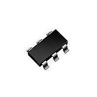
NCP1250ASN65T1G ON Semiconductor, NCP1250ASN65T1G Datasheet - Page 15

NCP1250ASN65T1G
Manufacturer Part Number
NCP1250ASN65T1G
Description
IC PWM CTLR OCP LATCH 6-TSOP
Manufacturer
ON Semiconductor
Datasheet
1.NCP1250ASN65T1G.pdf
(21 pages)
Specifications of NCP1250ASN65T1G
Output Isolation
Isolated
Frequency Range
61kHz ~ 71kHz
Voltage - Input
9.4 V ~ 28 V
Voltage - Output
12V
Operating Temperature
-40°C ~ 125°C
Package / Case
6-TSOP (0.063", 1.60mm Width)
Number Of Outputs
1
Duty Cycle (max)
84 %
Output Current
300 mA
Mounting Style
SMD/SMT
Switching Frequency
65 KHz
Operating Supply Voltage
28 V
Supply Current
2.1 mA
Maximum Operating Temperature
+ 125 C
Fall Time
30 ns
Minimum Operating Temperature
- 40 C
Rise Time
40 ns
Lead Free Status / RoHS Status
Lead free / RoHS Compliant
Available stocks
Company
Part Number
Manufacturer
Quantity
Price
Company:
Part Number:
NCP1250ASN65T1G
Manufacturer:
ON Semiconductor
Quantity:
1 250
Part Number:
NCP1250ASN65T1G
Manufacturer:
ON/安森美
Quantity:
20 000
characteristics:
V
V
N
N
Given the turns ratio between the primary and the auxiliary
windings, the on−time voltage at high line (265 Vac) on the
auxiliary winding swings down to:
install a divider featuring the following ratio:
protect the pin against ESD pulses. These diodes accept
some peak current in the avalanche mode and are designed
to sustain a certain amount of energy. On the other side,
negative injection into these diodes (or forward bias) can
cause substrate injection which can lead to an erratic circuit
behavior. To avoid this problem, the pin is internally
clamped slightly below –300 mV which means that if more
current is injected before reaching the ESD forward drop,
then the maximum peak reduction is kept to 40%. If the
voltage finally forward biases the internal zener diode, then
care must be taken to avoid injecting a current beyond
–2 mA. Given the value of R
present example.
fixes the maximum peak current set point to 0.8 V even if the
OPP pin is inadvertently biased above 0 V.
out
in
1
2
V
Let us assume that we have the following converter
To obtain a level as imposed by Equation 6, we need to
The OPP pin is surrounded by Zener diodes stacked to
Finally, please note that another comparator internally
aux
= N
= N
= 85 to 265 V
= 19 V
+ −N
p
p
:N
:N
s
aux
= 1:0.25
2
V
= 1:0.18
in,max
rms
+ −0.18
Figure 42. The Peak Current Regularly Reduces Down to 20% at 375 Vdc
100%
80%
Peak current
setpoint
OPPU
375 + −67.5 V
, there is no risk in the
(eq. 7)
http://onsemi.com
15
then the upper resistor can be obtained by:
implementing the recommended resistor values, we obtain
the following curve (Figure 42):
Frequency Foldback
the need for improving the efficiency, requires a change to
the traditional fixed−frequency type of operation. This
controller implements a switching frequency foldback when
the feedback voltage passes below a certain level, V
around 1.5 V. At this point, the oscillator enters frequency
foldback and reduces its switching frequency. The peak
current setpoint follows the feedback pin until its level
reaches 1.05 V. Below this value, the peak current freezes to
V
and the only way to further reduce the transmitted power is
to reduce the operating frequency down to 26 kHz. This
value is reached at a voltage feedback level of 350 mV
typically. Below this point, if the output power continues to
decrease, the part enters skip cycle for the best noise−free
performance in no−load conditions. Figure 43 depicts the
adopted scheme for the part.
fold
If we arbitrarily fix the pull−down resistor R
If we now plot the peak current set point obtained by
The reduction of no−load standby power associated with
/4.2 (250 mV or 31% of the maximum 0.8 V setpoint)
375
R
OPPU
Div +
+
67.5 * 0.16
0.16 1k
0.16
67.5
V
bulk
[ 2.4m
[ 421 kW
OPPL
to 1 kW,
fold
(eq. 8)
(eq. 9)
, set


