CP2105EK Silicon Laboratories Inc, CP2105EK Datasheet - Page 14
CP2105EK
Manufacturer Part Number
CP2105EK
Description
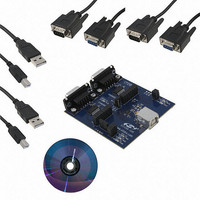
KIT EVAL FOR CP2105
Manufacturer
Silicon Laboratories Inc
Specifications of CP2105EK
Main Purpose
Interface, Dual USB 2.0 to UART (RS485) Bridge
Embedded
No
Utilized Ic / Part
CP2105
Primary Attributes
Full Speed (12Mbps)
Secondary Attributes
LED Status Indicators
Interface Type
RS-232, USB
Operating Supply Voltage
3.3 V
Product
Interface Development Tools
For Use With/related Products
CP2105
Lead Free Status / RoHS Status
Lead free / RoHS Compliant
Lead Free Status / RoHS Status
Lead free / RoHS Compliant
Other names
336-2005
Available stocks
Company
Part Number
Manufacturer
Quantity
Price
Company:

Part Number:
CP2105EK
Manufacturer:
SiliconL
Quantity:
15


CP2105
8. GPIO Pins
The CP2105 supports five user-configurable GPIO pins for status and control information. The Standard
Communication Interface (SCI) has three GPIO pins and the Enhanced Communication Interface (ECI) has two
GPIO pins. To use the pins as GPIO pins, the interface with the GPIO pins must be configured in GPIO Mode. By
default, both communication interfaces on the CP2105 are configured for GPIO Mode. If the Modem Control
signals are needed, the interface must be configured for Modem Mode. See Section 7 for more information on
Modem Mode.
Each of these GPIO pins are usable as inputs, open-drain outputs, or push-pull outputs. Four of the GPIO pins also
have alternate functions listed in Table 12 (GPIO.2_SCI does not have an alternate function).
By default, all of the GPIO pins are configured as a GPIO input. The configuration of the pins is one-time
programmable for each device. The difference between an open-drain output and a push-pull output is when the
GPIO output is driven to logic high. A logic high, open-drain output pulls the pin to the VIO rail through an internal,
pull-up resistor. A logic high, push-pull output directly connects the pin to the VIO voltage. Open-drain outputs are
typically used when interfacing to logic at a higher voltage than the VIO pin. These pins can be safely pulled to the
higher, external voltage through an external pull-up resistor. The maximum external pull-up voltage is 5 V.
The speed of reading and writing the GPIO pins is subject to the timing of the USB bus. GPIO pins configured as
inputs or outputs are not recommended for real-time signalling.
More information regarding the configuration and usage of these pins can be found in “AN144: CP21xx
Customization Guide” and “AN223: Port Configuration and GPIO for CP210x” available on the Silicon Labs
website.
8.1. GPIO.0-1—Transmit and Receive Toggle
GPIO.0 and GPIO.1 are configurable as Transmit Toggle and Receive Toggle pins for both the Enhanced
Communication Interface and the Standard Communication Interface. These pins are logic high when a device is
not transmitting or receiving data, and they toggle at a fixed rate as specified in Table 6 when data transfer is in
progress. Typically, these pins are connected to two LEDs to indicate data transfer.
14
Figure 5. Transmit and Receive Toggle Typical Connection Diagram
GPIO.0_ECI
GPIO.1_ECI
GPIO.0_SCI
GPIO.1_SCI
GPIO Pin
Table 12. GPIO Mode Alternate Functions
GPIO.1 – RX Toggle
GPIO.0 – TX Toggle
CP2105
RX Toggle/RS-485 Transceiver Control
Rev. 1.0
Alternate Function
RX Toggle
TX Toggle
TX Toggle
VIO
Related parts for CP2105EK
Image
Part Number
Description
Manufacturer
Datasheet
Request
R

Part Number:
Description:
QFN 24/I°/USB TO DUAL UART BRIDGE
Manufacturer:
Silicon Laboratories Inc

Part Number:
Description:
IC SGL USB-DL UART BRIDGE 24QFN
Manufacturer:
Silicon Laboratories Inc
Datasheet:
Part Number:
Description:
SMD/C°/SINGLE-ENDED OUTPUT SILICON OSCILLATOR
Manufacturer:
Silicon Laboratories Inc
Part Number:
Description:
Manufacturer:
Silicon Laboratories Inc
Datasheet:
Part Number:
Description:
N/A N/A/SI4010 AES KEYFOB DEMO WITH LCD RX
Manufacturer:
Silicon Laboratories Inc
Datasheet:
Part Number:
Description:
N/A N/A/SI4010 SIMPLIFIED KEY FOB DEMO WITH LED RX
Manufacturer:
Silicon Laboratories Inc
Datasheet:
Part Number:
Description:
N/A/-40 TO 85 OC/EZLINK MODULE; F930/4432 HIGH BAND (REV E/B1)
Manufacturer:
Silicon Laboratories Inc
Part Number:
Description:
EZLink Module; F930/4432 Low Band (rev e/B1)
Manufacturer:
Silicon Laboratories Inc
Part Number:
Description:
I°/4460 10 DBM RADIO TEST CARD 434 MHZ
Manufacturer:
Silicon Laboratories Inc
Part Number:
Description:
I°/4461 14 DBM RADIO TEST CARD 868 MHZ
Manufacturer:
Silicon Laboratories Inc
Part Number:
Description:
I°/4463 20 DBM RFSWITCH RADIO TEST CARD 460 MHZ
Manufacturer:
Silicon Laboratories Inc
Part Number:
Description:
I°/4463 20 DBM RADIO TEST CARD 868 MHZ
Manufacturer:
Silicon Laboratories Inc
Part Number:
Description:
I°/4463 27 DBM RADIO TEST CARD 868 MHZ
Manufacturer:
Silicon Laboratories Inc
Part Number:
Description:
I°/4463 SKYWORKS 30 DBM RADIO TEST CARD 915 MHZ
Manufacturer:
Silicon Laboratories Inc