HT13CB103JN Kemet, HT13CB103JN Datasheet - Page 40
HT13CB103JN
Manufacturer Part Number
HT13CB103JN
Description
Multilayer Ceramic Capacitors (MLCC) - Leaded HT13 0.01uF 100volts X7R 5%
Manufacturer
Kemet
Series
HTr
Datasheet
1.HT13CN471KN.pdf
(53 pages)
Specifications of HT13CB103JN
Voltage Rating
100 Volts
Termination Style
Axial
Operating Temperature Range
- 55 C to + 200 C
Product
High Temperature MLCCs
Dimensions
3.43 mm Dia. x 6.6 mm L
Capacitance
0.01 uF
Tolerance
5 %
Temperature Coefficient
X7R
Lead Free Status / RoHS Status
Lead free / RoHS Compliant


1. The ceramic chip capacitors described in this section are the types used
2. Types BP available as described in MIL-PRF-49467.
3. Group A and B screening per MIL-PRF-49467 available. - TCVC exceptions apply.
4. Ceramic chip capacitors are extremely sensitive to thermal shock damage
5. Higher voltages available upon request.
6. Where nickel barrier termination is required, bandwidth dimensions
in our other high voltage ceramic multilayer product lines.
during installation. Wherever possible, processes involving infrared or
vapor phase soldering systems should be utilized.
may exceed the standard dimension listed.
Chip Size
1515
1812
1825
2020
2225
2520
3333
3530
4040
4540
5440
5550
6560
FEATURES
Style
1515
1812
1825
2020
2225
2520
3333
3530
4040
4540
5440
5550
6560
T (Total Length)
10.91
12.88
14.21
16.51
18.92
19.80
11.51
5390
5.20
5.90
6.50
7.00
8.68
© KEMET Electronics Corporation • PO Box 5928 • Greenville, SC 29606 • www.kemet.com
mm
Style
1515, 2020, etc.
Dielectric
B or R = X7R
N = C0G (NP0)
Capacitance Value
First two digits are significant,
last digit is number of zeros,
i.e., 472=4700pF
Tolerance
J = ±5% C0G (NP0)
K = ±10%
M = ±20%
P = 0/+100%
Z = -20%/+80%
0.205
0.232
0.232
0.256
0.276
0.342
0.430
0.453
0.507
0.559
0.650
0.745
0.780
4540
in.
.450 ±.030 (11.43 ±.76)
.150 ±.015 (3.81 ±.38)
.180 ±.020 (4.57 ±.51)
.180 ±.020 (4.57 ±.51)
.200 ±.020 (5.08 ±.51)
.220 ±.020 (5.59 ±.51)
.250 ±.020 (6.35 ±.51)
.330 ±.030 (8.38 ±.76)
.350 ±.030 (8.89 ±.76)
.400 ±.030 (10.2 ±.76)
.540 ±.030 (13.7 ±.76)
.550 ±.030 (14.0 ±.76)
.650 ±.030 (16.5 ±.76)
RECOMMENDED SOLDER PAD PATTERN DIMENSIONS
PART NUMBER AND ORDERING INFORMATION
Inches (mm)
Length (L)
10.15
10.41
12.82
13.20
S (Separation)
1.90
2.30
2.30
2.80
3.30
4.98
7.11
7.61
8.88
mm
B
Ceramic Chip (+125°C)
0.075
0.091
0.091
0.130
0.196
0.280
0.300
0.350
0.400
0.410
0.505
0.520
0.110
in.
472
Military Equivalent
As required by customer only.
DIMENSIONS
11.05
11.05
11.05
13.59
16.13
W (Pad Width)
4.34
3.70
6.90
5.62
6.80
5.62
9.27
8.51
mm
High Voltage
.150 ±.015 (3.81 ±.38)
.120 ±.015 (3.05 ±.38)
.250 ±.020 (6.35 ±.51)
.200 ±.020 (5.08 ±.51)
.250 ±.020 (6.35 ±.51)
.200 ±.020 (5.08 ±.51)
.330 ±.030 (8.38 ±.76)
.300 ±.030 (7.62 ±.76)
.400 ±.030 (10.2 ±.76)
.400 ±.030 (10.2 ±.76)
.400 ±.030 (10.2 ±.76)
.500 ±.030 (12.7 ±.76)
.600 ±.030 (15.2 ±.76)
Not applicable
0.171
0.146
0.272
0.221
0.268
0.221
0.365
0.335
0.435
0.435
0.435
0.535
0.635
Inches (mm)
in.
M
MARKING
Width (W)
L (Pad Length)
1.65
1.80
1.80
1.85
1.85
1.85
1.90
1.95
2.00
2.03
3.05
3.05
3.30
mm
202
0.065
0.071
0.071
0.073
0.073
0.073
0.075
0.077
0.079
0.080
0.120
0.120
0.130
in.
Thickness (T) max
P
Inches (mm)
.140 (3.55)
.100 (2.54)
.160 (4.07)
.180 (3.55)
.200 (5.08)
.180 (4.57)
.220 (5.59)
.220 (5.59)
.220 (5.59)
.220 (5.59)
.220 (5.59)
.220 (5.59)
.220 (5.59)
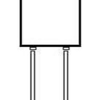
CERAMIC CHIP OUTLINE DRAWING
M
Voltage
First two digits are significant,
last digit is number of zeros,
i.e., 202=2000V
Terminal Material
P = PdAg
S = Ag
E = Ag/Ni/SnPb Plate
C = Ag/Ni/Sn Plate
Group A Screening*
Add to part number if required
*MIL-PRF-49467
(subgroup 1)
except Corona
L
Bandwidth (BW)
.010 - .030”
.010 - .040”
.010 - .040”
.010 - .040”
.010 - .040”
.030 - .060”
.030 - .060”
.030 - .060”
.030 - .060”
.030 - .060”
.030 - .060”
.030 - .060”
.030 - .060”
Inches
T
S
L
39
Related parts for HT13CB103JN
Image
Part Number
Description
Manufacturer
Datasheet
Request
R

Part Number:
Description:
Rectifiers 1.0 Amp 200 Volt 30 Amp IFSM
Manufacturer:
Taiwan Semiconductor
Datasheet:

Part Number:
Description:
CAP, KEMET #F601BL105K250C
Manufacturer:
Kemet
Datasheet:
Part Number:
Description:
Manufacturer:
Kemet
Datasheet:
Part Number:
Description:
Manufacturer:
Kemet
Datasheet: