ADXL345BCCZ Analog Devices Inc, ADXL345BCCZ Datasheet - Page 26
ADXL345BCCZ
Manufacturer Part Number
ADXL345BCCZ
Description
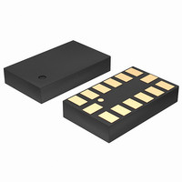
IC ACCEL SPI/I2C 3AX 3G 14LGA
Manufacturer
Analog Devices Inc
Series
iMEMS®r
Datasheet
1.EVAL-ADXL345Z.pdf
(40 pages)
Specifications of ADXL345BCCZ
Acceleration Range
±2g, 4g, 8g, 16g
Design Resources
Sensing Low-g Acceleration Using ADXL345 Digital Accelerometer Connected to ADuC7024 (CN0133)
Axis
X, Y, Z
Sensitivity
256LSB/g, 128LSB/g, 64LSB/g, 32LSB/g
Voltage - Supply
2 V ~ 3.6 V
Output Type
Digital
Bandwidth
6.25Hz ~ 3.2kHz Selectable
Interface
I²C, SPI
Mounting Type
Surface Mount
Package / Case
14-LGA
No. Of Axes
3
Sensor Case Style
LGA
No. Of Pins
14
Supply Voltage Range
2V To 3.6V
Operating Temperature Range
-40°C To +85°C
Package
14LGA
Acceleration
±2/±4/±8/±16 g
Axis Type
Triple
Operating Supply Voltage
2 to 3.6 V
Mounting
Surface Mount
Lead Free Status / RoHS Status
Lead free / RoHS Compliant
For Use With
EVAL-ADXL345Z - BOARD EVALUATION FOR ADXL345EVAL-ADXL345Z-S - BOARD SATELLITE FOR ADXL345Z-MEVAL-ADXL345Z-M - BOARD EVAL FOR ADXL345
Lead Free Status / RoHS Status
Lead free / RoHS Compliant, Lead free / RoHS Compliant
Other names
Q4372599
Available stocks
Company
Part Number
Manufacturer
Quantity
Price
Company:

Part Number:
ADXL345BCCZ
Manufacturer:
ADI
Quantity:
10
Company:
Part Number:
ADXL345BCCZ
Manufacturer:
AD
Quantity:
828
Part Number:
ADXL345BCCZ
Manufacturer:
ADI/亚德诺
Quantity:
20 000
Company:
Part Number:
ADXL345BCCZ-RL7
Manufacturer:
POWER
Quantity:
14 300


ADXL345
If the link bit is not set, the AUTO_SLEEP feature is disabled
and setting the AUTO_SLEEP bit does not have an impact on
device operation. Refer to the Link Bit section or the Link Mode
section for more information on utilization of the link feature.
When clearing the AUTO_SLEEP bit, it is recommended that the
part be placed into standby mode and then set back to measure-
ment mode with a subsequent write. This is done to ensure that
the device is properly biased if sleep mode is manually disabled;
otherwise, the first few samples of data after the AUTO_SLEEP
bit is cleared may have additional noise, especially if the device
was asleep when the bit was cleared.
Measure Bit
A setting of 0 in the measure bit places the part into standby mode,
and a setting of 1 places the part into measurement mode. The
ADXL345 powers up in standby mode with minimum power
consumption.
Sleep Bit
A setting of 0 in the sleep bit puts the part into the normal mode
of operation, and a setting of 1 places the part into sleep mode.
Sleep mode suppresses DATA_READY, stops transmission of data
to FIFO, and switches the sampling rate to one specified by the
wakeup bits. In sleep mode, only the activity function can be used.
When the DATA_READY interrupt is suppressed, the output
data registers (Register 0x32 to Register 0x37) are still updated
at the sampling rate set by the wakeup bits (D1:D0).
When clearing the sleep bit, it is recommended that the part be
placed into standby mode and then set back to measurement
mode with a subsequent write. This is done to ensure that the
device is properly biased if sleep mode is manually disabled;
otherwise, the first few samples of data after the sleep bit is
cleared may have additional noise, especially if the device was
asleep when the bit was cleared.
Wakeup Bits
These bits control the frequency of readings in sleep mode as
described in Table 20.
Table 20. Frequency of Readings in Sleep Mode
D1
0
0
1
1
Setting
D0
0
1
0
1
Frequency (Hz)
8
4
2
1
Rev. B | Page 26 of 40
Register 0x2E—INT_ENABLE (Read/Write)
D7
DATA_READY
D3
Inactivity
Setting bits in this register to a value of 1 enables their respective
functions to generate interrupts, whereas a value of 0 prevents
the functions from generating interrupts. The DATA_READY,
watermark, and overrun bits enable only the interrupt output;
the functions are always enabled. It is recommended that interrupts
be configured before enabling their outputs.
Register 0x2F—INT_MAP (R/ W )
D7
DATA_READY
D3
Inactivity
Any bits set to 0 in this register send their respective interrupts to
the INT1 pin, whereas bits set to 1 send their respective interrupts
to the INT2 pin. All selected interrupts for a given pin are OR’ e d.
Register 0x30—INT_SOURCE (Read Only)
D7
DATA_READY
D3
Inactivity
Bits set to 1 in this register indicate that their respective functions
have triggered an event, whereas a value of 0 indicates that the
corresponding event has not occurred. The DATA_READY,
watermark, and overrun bits are always set if the corresponding
events occur, regardless of the INT_ENABLE register settings,
and are cleared by reading data from the DATAX, DATAY, and
DATAZ registers. The DATA_READY and watermark bits may
require multiple reads, as indicated in the FIFO mode descriptions
in the FIFO section. Other bits, and the corresponding interrupts,
are cleared by reading the INT_SOURCE register.
Register 0x31—DATA_FORMAT (Read/Write)
D7
SELF_TEST
The DATA_FORMAT register controls the presentation of data
to Register 0x32 through Register 0x37. All data, except that for
the ±16 g range, must be clipped to avoid rollover.
SELF_TEST Bit
A setting of 1 in the SELF_TEST bit applies a self-test force to
the sensor, causing a shift in the output data. A value of 0 disables
the self-test force.
SPI Bit
A value of 1 in the SPI bit sets the device to 3-wire SPI mode,
and a value of 0 sets the device to 4-wire SPI mode.
D6
SPI
D5
INT_INVERT
D6
SINGLE_TAP
D2
FREE_FALL
D6
SINGLE_TAP
D2
FREE_FALL
D6
SINGLE_TAP
D2
FREE_FALL
D4
0
D5
DOUBLE_TAP
D1
Watermark
D5
DOUBLE_TAP
D1
Watermark
D5
DOUBLE_TAP
D1
Watermark
D3
FULL_RES
D2
Justify
D4
Activity
D0
Overrun
D4
Activity
D0
Overrun
D4
Activity
D0
Overrun
D1
Range
D0
Related parts for ADXL345BCCZ
Image
Part Number
Description
Manufacturer
Datasheet
Request
R

Part Number:
Description:
±1.7g Dual-Axis IMEMS Accelerometer Evaluation Board
Manufacturer:
Analog Devices Inc
Datasheet:

Part Number:
Description:
Inertial Sensor Evaluation System
Manufacturer:
Analog Devices Inc
Datasheet:
Part Number:
Description:
Manufacturer:
Analog Devices Inc
Datasheet:
Part Number:
Description:
Manufacturer:
Analog Devices Inc
Datasheet:
Part Number:
Description:
Manufacturer:
Analog Devices Inc
Datasheet:
Part Number:
Description:
Manufacturer:
Analog Devices Inc
Datasheet:
Part Number:
Description:
Manufacturer:
Analog Devices Inc
Datasheet:
Part Number:
Description:
Manufacturer:
Analog Devices Inc
Datasheet:
Part Number:
Description:
Manufacturer:
Analog Devices Inc
Datasheet:
Part Number:
Description:
Manufacturer:
Analog Devices Inc
Datasheet:
Part Number:
Description:
Manufacturer:
Analog Devices Inc
Datasheet:
Part Number:
Description:
Manufacturer:
Analog Devices Inc
Datasheet:
Part Number:
Description:
Manufacturer:
Analog Devices Inc
Datasheet: