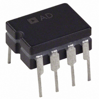
OP249FZ Analog Devices Inc, OP249FZ Datasheet

OP249FZ
Specifications of OP249FZ
Available stocks
Related parts for OP249FZ
OP249FZ Summary of contents
Page 1
FEATURES Fast slew rate: 22 V/μs typical Settling time (0.01%): 1.2 μs maximum Offset voltage: 200 μV typical High open-loop gain: 1000 V/mV minimum Low total harmonic distortion: 0.002% typical APPLICATIONS Output amplifier for fast DACs Signal processing Instrumentation amplifiers ...
Page 2
OP249 TABLE OF CONTENTS Features .............................................................................................. 1 Applications ....................................................................................... 1 Pin Configurations ........................................................................... 1 General Description ......................................................................... 1 Revision History ............................................................................... 2 Specifications ..................................................................................... 3 Electrical Characteristics ............................................................. 3 Absolute Maximum Ratings ............................................................ 6 ESD Caution .................................................................................. 6 REVISION HISTORY ...
Page 3
SPECIFICATIONS ELECTRICAL CHARACTERISTICS V = ± 25°C, unless otherwise noted Table 1. Parameter Symbol Offset Voltage V OS Offset Stability Input Bias Current I B Input Offset Current Input Voltage Range IVR ...
Page 4
OP249 V = ± 25°C, unless otherwise noted Table 2. Parameter Symbol Offset Voltage V OS Input Bias Current I B Input Offset Current Input Voltage Range IVR Common-Mode Rejection CMR Power ...
Page 5
V = ±15 V, −55°C ≤ T ≤ +125°C for A grade, unless otherwise noted Table 3. Parameter Offset Voltage Offset Voltage Temperature Coefficient 1 Input Bias Current 1 Input Offset Current Input Voltage Range 2 Common-Mode Rejection ...
Page 6
OP249 ABSOLUTE MAXIMUM RATINGS Table 5. 1 Parameter Supply Voltage 2 Input Voltage 2 Differential Input Voltage Output Short-Circuit Duration Storage Temperature Range Operating Temperature Range OP249A (Q) OP249F (Q) OP249G (N, R) Junction Temperature Range OP249A (Q), OP249F (Q) ...
Page 7
TYPICAL PERFORMANCE CHARACTERISTICS 120 T = 25° ±15V S 100 R = 2kΩ GAIN 40 PHASE 20 0 –20 1k 10k 100k 1M FREQUENCY (Hz) Figure 6. Open-Loop Gain, Phase vs. Frequency 65 V ...
Page 8
OP249 25° ±15V NEGATIVE 20 POSITIVE 100 200 300 CAPACITIVE LOAD (pF) Figure 12. Slew Rate vs. Capacitive Load 25° ...
Page 9
Figure 18. Distortion vs. Frequency 0.1 0.01 20 100 1k Figure 19. Distortion vs. Frequency 0.1 0.01 20 100 1k Figure 20. Distortion vs. Frequency 500mV T = 25° ±15V S V ...
Page 10
OP249 OP249 5 AD712 FREQUENCY (Hz) Figure 24. Output Voltage vs. Frequency ±15V 2kΩ 100mV p ...
Page 11
T = 25°C A 160 V = ±15V S 415 × OP249 (830 OP AMPS) 140 120 100 –1000 –800 –600 –400 –200 0 200 400 V (µV) OS Figure 30. V Distribution (N-8) ...
Page 12
OP249 25° –75 –50 – TEMPERATURE (°C) Figure 36. Input Offset Current vs. Temperature 12000 V = ±15V S 10000 8000 R = 10kΩ L 6000 ...
Page 13
APPLICATIONS INFORMATION +IN –IN Figure 39. Simplified Schematic (1/2 OP249) 2 1/2 1 OP249 +3V 3 +18V 6 8 1/2 7 OP249 + –18V Figure 40. Burn-In Circuit The OP249 represents a reliable JFET amplifier design, featuring an ...
Page 14
OP249 100 50mV Figure 42. Small-Signal Transient Response kΩ||100 pF, No Compensation with most JFET input amplifiers, the output of the OP249 can undergo phase inversion if ...
Page 15
DAC OUTPUT AMPLIFIER Unity-gain stability, a low offset voltage of 300 μV typical, and a fast settling time of 870 ns to 0.01%, makes the OP249 an ideal amplifier for fast DACs. For CMOS DAC applications, the low offset voltage ...
Page 16
OP249 100 500mV C = 5pF RESPONSE IS GROSSLY UNDERDAMPED, AND EXHIBITS RINGING Figure 49. Effect of Altering Compensation from Circuit in Figure 47—PM7545 CMOS DAC with 1/2 OP249, Unipolar Operation; Figure 49 illustrates the effect of ...
Page 17
OUTLINE DIMENSIONS 0.210 (5.33) MAX 0.150 (3.81) 0.130 (3.30) 0.115 (2.92) 0.022 (0.56) 0.018 (0.46) 0.014 (0.36) CONTROLLING DIMENSIONS ARE IN INCHES; MILLIMETER DIMENSIONS (IN PARENTHESES) ARE ROUNDED-OFF INCH EQUIVALENTS FOR REFERENCE ONLY AND ARE NOT APPROPRIATE FOR USE IN ...
Page 18
... OP249 ORDERING GUIDE Model 1 Temperature Range OP249AZ −55°C to +125°C OP249FZ −40°C to +85°C OP249GP −40°C to +85°C OP249GPZ −40°C to +85°C OP249GS −40°C to +85°C OP249GS-REEL −40°C to +85°C OP249GS-REEL7 −40°C to +85°C OP249GSZ − ...
Page 19
NOTES Rev Page OP249 ...
Page 20
OP249 NOTES ©1989–2010 Analog Devices, Inc. All rights reserved. Trademarks and registered trademarks are the property of their respective owners. D00296-0-4/10(G) Rev Page ...


