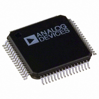
AD9238BST-40 Analog Devices Inc, AD9238BST-40 Datasheet - Page 9

AD9238BST-40
Manufacturer Part Number
AD9238BST-40
Description
IC, ADC, 12BIT, 40MSPS, QFP-64
Manufacturer
Analog Devices Inc
Datasheet
1.AD9238BSTZ-40.pdf
(48 pages)
Specifications of AD9238BST-40
Resolution (bits)
12bit
Sampling Rate
40MSPS
Input Channel Type
Differential
Data Interface
Parallel
Supply Voltage Range - Analog
2.7V To 3.6V
Supply Current
110mA
Digital Ic Case Style
QFP
Rohs Status
RoHS non-compliant
Number Of Bits
12
Sampling Rate (per Second)
40M
Number Of Converters
2
Power Dissipation (max)
330mW
Voltage Supply Source
Single Supply
Operating Temperature
-40°C ~ 85°C
Mounting Type
Surface Mount
Package / Case
64-LQFP
Lead Free Status / RoHS Status
Contains lead / RoHS non-compliant
For Use With
AD9238BCP-65EBZ - BOARD EVAL WITH AD9238BCP-65AD9238BCP-40EBZ - BOARD EVAL WITH AD9238BCP-40
Lead Free Status / RoHS Status
Contains lead / RoHS non-compliant
Available stocks
Company
Part Number
Manufacturer
Quantity
Price
Company:
Part Number:
AD9238BST-40
Manufacturer:
ADI
Quantity:
300
Company:
Part Number:
AD9238BST-40
Manufacturer:
Analog Devices Inc
Quantity:
10 000
Table 6. 64-Lead LQFP and 64-Lead LFCSP Pin Function Descriptions
Pin No.
1, 4, 13, 16
2
3
5, 12, 17, 64
6
7
8
9
10
11
14
15
18
19
20
21
22
23, 24, 42, 43
25 to 27,
30 to 38
28, 40, 53
29, 41, 52
39
44 to 51,
54 to 57
58
59
60
61
62
63
Mnemonic
AGND
VIN+_A
VIN–_A
AVDD
REFT_A
REFB_A
VREF
SENSE
REFB_B
REFT_B
VIN−_B
VIN+_B
CLK_B
DCS
DFS
PDWN_B
OEB_B
DNC
D0_B (LSB) to
D11_B (MSB)
DRGND
DRVDD
OTR_B
D0_A (LSB) to
D11_A (MSB)
OTR_A
OEB_A
PDWN_A
MUX_SELECT
SHARED_REF
CLK_A
EP
Description
Analog Ground.
Analog Input Pin (+) for Channel A.
Analog Input Pin (−) for Channel A.
Analog Power Supply.
Differential Reference (+) for Channel A.
Differential Reference (−) for Channel A.
Voltage Reference Input/Output.
Reference Mode Selection.
Differential Reference (−) for Channel B.
Differential Reference (+) for Channel B.
Analog Input Pin (−) for Channel B.
Analog Input Pin (+) for Channel B.
Clock Input Pin for Channel B.
Enable Duty Cycle Stabilizer (DCS) Mode (Tie High to Enable).
Data Output Format Select Bit (Low for Offset Binary, High for Twos Complement).
Output Enable Bit for Channel B:
Do Not Connect Pins. Should be left floating.
Channel B Data Output Bits.
Digital Output Ground.
Digital Output Driver Supply. Must be decoupled to DRGND with a minimum 0.1 μF capacitor.
Recommended decoupling is 0.1 μF capacitor in parallel with 10 μF.
Out-of-Range Indicator for Channel B.
Channel A Data Output Bits.
Out-of-Range Indicator for Channel A.
Output Enable Bit for Channel A:
Power-Down Function Selection for Channel A:
Data Multiplexed Mode. (See Data Format section for how to enable; high setting disables
output data multiplexed mode).
Shared Reference Control Bit (Low for Independent Reference Mode, High for Shared
Reference Mode).
Clock Input Pin for Channel A.
For the 64-Lead LFCSP only, there is an exposed pad that must connect to AGND.
Power-Down Function Selection for Channel B:
Logic 0 enables Data Bus B.
Logic 1 sets outputs to High-Z.
Logic 0 enables Data Bus A.
Logic 1 sets outputs to High-Z.
Logic 0 enables Channel A.
Logic 1 powers down Channel A. (Outputs static, not High-Z.)
Logic 0 enables Channel B.
Logic 1 powers down Channel B. (Outputs static, not High-Z.)
Rev. C | Page 9 of 48
AD9238


