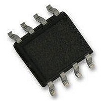
WM8727GED/RV Wolfson Microelectronics, WM8727GED/RV Datasheet - Page 14

WM8727GED/RV
Manufacturer Part Number
WM8727GED/RV
Description
IC, DAC, STEREO, 24BIT, 8SOIC
Manufacturer
Wolfson Microelectronics
Datasheets
1.WM8727GEDRV.pdf
(16 pages)
2.WM8727GEDRV.pdf
(16 pages)
3.WM8727GEDRV.pdf
(17 pages)
4.WM8727GEDRV.pdf
(16 pages)
Specifications of WM8727GED/RV
Resolution (bits)
24bit
Supply Voltage Range - Analogue
2.7V To 5.5V
Supply Current
27mA
No. Of Pins
8
Operating Temperature Range
-40°C To +85°C
Svhc
No SVHC (15-Dec-2010)
Data Interface
Serial
Sampling Rate
192kSPS
Input Channel Type
Serial
Digital Ic Case Style
SOIC
Rohs Compliant
Yes
Lead Free Status / RoHS Status
Lead free / RoHS Compliant
Available stocks
Company
Part Number
Manufacturer
Quantity
Price
Company:
Part Number:
WM8727GED/RV
Manufacturer:
NS
Quantity:
549
Part Number:
WM8727GED/RV
Manufacturer:
WM
Quantity:
20 000
WM8727
RECOMMENDED ANALOGUE LOW PASS FILTER (OPTIONAL)
Figure 11 Recommended Low Pass Filter (Optional)
PCB LAYOUT RECOMMENDATIONS
w
+
10uF
47k
1.8k
An external low pass filter is recommended (see Figure 20) if the device is driving a wideband
amplifier. In some applications, a passive RC filter may be adequate.
Care should be taken in the layout of the PCB that the WM8727 is to be mounted to. The
following notes will help in this respect:
1.
2.
3.
An evaluation board is available for the WM8727 that demonstrates the above techniques and
the excellent performance achievable from the device. This can be ordered or the User manual
downloaded from the Wolfson web site at
1.0nF
4.7k
7.5K
The VDD supply to the device should be as noise free as possible. This can be
accomplished to a large degree with a 10uF bulk capacitor placed locally to the device and a
0.1uF high frequency decoupling capacitor placed as close to the VDD pin as possible. It is
best to place the 0.1uF capacitor directly between the VDD and GND pins of the device on
the same layer to minimize track inductance and thus improve device decoupling
effectiveness.
Separate analogue and digital track routing from each other. The device is split into
analogue (pins 5 – 8) and digital (pins 1 – 4) sections that allow the routing of these signals
to be easily separated. By physically separating analogue and digital signals, crosstalk from
the PCB can be minimized.
Use an unbroken solid GND plane.
advisable to have either a GND plane layer on a multilayer PCB or to dedicate one side of a
2 layer PCB to be a GND plane. For double sided implementations it is best to route as
many signals as possible on the device mounted side of the board, with the opposite side
acting as a GND plane. The use of a GND plane greatly reduces any electrical emissions
from the PCB and minimizes crosstalk between signals.
4.7k
680pF
_
+
+VS
-VS
51
www.wolfsonmicro.com
To achieve best performance from the device, it is
PD Rev 4.2 July 2006
Production Data
14


