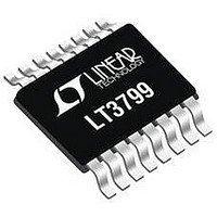
LT3799IMSE#PBF Linear Technology, LT3799IMSE#PBF Datasheet - Page 7

LT3799IMSE#PBF
Manufacturer Part Number
LT3799IMSE#PBF
Description
IC, LED DRVR, MSOP-16
Manufacturer
Linear Technology
Datasheet
1.LT3799EMSEPBF.pdf
(20 pages)
Specifications of LT3799IMSE#PBF
Led Driver Application
High Power LED Driver, Automotive Lighting
No. Of Outputs
1
Output Current
3A
Input Voltage
18V
Dimming Control Type
Analog
Topology
Flyback
Rohs Compliant
Yes
Lead Free Status / RoHS Status
Lead free / RoHS Compliant
Available stocks
Company
Part Number
Manufacturer
Quantity
Price
PIN FUNCTIONS
V
the internal start-up circuitry and to the INTV
pin must be locally bypassed with a capacitor. A 25V shunt
regulator is internally connected to this pin.
INTV
and GATE Driver. Supplied from V
(typical). INTV
placed close to the pin.
COMP
Internal Error Amplifier. Connect a capacitor between these
two pins to compensate the internal feedback loop.
DCM (Pin 10): Discontinuous Conduction Mode Detection
Pin. Connect a capacitor and resistor in series with this
pin to the third winding.
V
for sensing the AC line voltage to perform power factor
correction. Connect the output of a resistor divider from
the line voltage to this pin. The voltage on this pin should
be between 1.25V to 1.5V at the maximum input voltage.
CTRL1, CTRL2, CTRL3 (Pin 1, Pin 2, Pin 3): Current Output
Adjustment Pins. These pins control the output current.
The lowest value of the three CTRL inputs is compared to
the negative input of the operational amplifier. Due to the
unique nature of the LT3799 control loop, the maximum
current does not directly correspond to the V
SENSE (Pin 15): The Current Sense Input for the Control
Loop. Kelvin connect this pin to the positive terminal of
the switch current sense resistor, R
of the N-channel MOSFET. The negative terminal of the
current sense resistor should be connected to the GND
plane close to the IC.
IN
IN_SENSE
(Pin 11): Input Voltage. This pin supplies current to
CC
+
, COMP
(Pin 13): Regulated Supply for Internal Loads
(Pin 16): Line Voltage Sense Pin. The pin is used
CC
–
must be bypassed with a 4.7μF capacitor
(Pin 7, Pin 8): Compensation Pins for
IN
SENSE
and regulates to 10V
, and the source
CTRL
CC
LDO. This
voltages.
GATE (Pin 14): N-Channel MOSFET Gate Driver Output.
Switches between INTV
GND during shutdown state.
FB (Pin 9): Voltage Loop Feedback Pin. FB is used to
detect open LED conditions by sampling the third winding
voltage. An open LED condition is reported if the CT pin
and the FB pin are higher than 1.25V.
CT (Pin 6): Timer Fault Pin. A capacitor is connected
between this pin and ground to provide an internal timer
for fault operations. During start-up, this pin is pulled to
ground and then charged with a 10μA current. Faults related
to the FB pin will be ignored until the CT pin reaches 1.25V.
If a fault is detected, the controller will stop switching and
begin to discharge the CT capacitor with a 200nA pull-down
current. When the pin reaches 240mV, the controller will
start to switch again.
FAULT (Pin 5): Fault Pin. An open-collector pull-down on
FAULT asserts if FB is greater than 1.25V with the CT pin
higher than 1.25V.
V
This pin drives a resistor divider for the CTRL pin, either
for analog dimming or for temperature limit/compensation
of LED load. Can supply up to 200μA.
GND (Exposed Pad Pin 17): Ground. The exposed pad
of the package provides both electrical contact to ground
and good thermal contact to the printed circuit board.
The exposed pad must be soldered to the circuit board
for proper operation.
REF
(Pin 4): Voltage Reference Output Pin, Typically 2V.
CC
and GND. This pin is pulled to
LT3799
7
3799f


