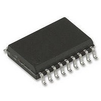
CAT310W-T1 CATALYST SEMICONDUCTOR, CAT310W-T1 Datasheet - Page 5

CAT310W-T1
Manufacturer Part Number
CAT310W-T1
Description
IC, LED DRIVER, LINEAR, SOIC-20
Manufacturer
CATALYST SEMICONDUCTOR
Datasheet
1.CAT310W-T1.pdf
(10 pages)
Specifications of CAT310W-T1
Led Driver Application
Automotive Lighting, LED Cluster Displays
No. Of Outputs
10
Output Current
50mA
Output Voltage
17V
Input Voltage
3V To 5.5V
Topology
Linear
Lead Free Status / RoHS Status
Lead free / RoHS Compliant
PIN DESCRIPTIONS
VCC is the supply input for the internal logic and is
compatible with both 3.3 V and 5 V systems. The logic is
held in a reset state until VCC exceeds 2.5 V. It is
recommended that a small bypass ceramic capacitor (1 mF)
be placed between VCC and GND pins on the device.
SIN is the CMOS logic pin for delivering the serial input
data stream into the internal 10−bit shift register. The most
recent or last data value in the serial stream is used to
configure the state of output channel “zero” (OUT0). During
the initial power up sequence all contents of the shift register
are reset and cleared to zero.
SCLK is the CMOS logic pin used to clock the internal shift
register. On each rising edge of clock, the serial data will
advance through one stage of the shift register.
XLAT is the CMOS logic input used to transfer data from
the 10−bit shift register into the output channel latches. An
internal pull−down current of 10 microampere is present on
this pin. When XLAT is low, the state of each output channel
remains unchanged. When XLAT is driven high, the
contents of the shift register appear at their respective output
channels. An external pull−up resistance of 10 kW or less is
adequate for logic high.
PGND, GND pins should be connected to the ground on the
PCB.
Table 5. PIN TABLE
Pin Number
11−15
6−10
16
17
18
19
20
1
2
3
4
5
OUT4 − OUT0
OUT9 − OUT5
Pin Name
BLANK
VBATT
PGND
SOUT
SCLK
XLAT
GND
VCC
N.C.
SIN
Clock input for the data shift register.
Control input for the data latch.
Serial data input.
Serial data output.
Ground.
Open drain outputs.
Open drain outputs.
Ground for LED driver outputs.
Battery sense input.
Power supply voltage for the logic
Blank input. When BLANK is high, all the output drivers are turned off.
No connect.
http://onsemi.com
5
BLANK is the CMOS logic input (active high) used to
temporarily disable all outputs. An internal pull−up current
of 10 microampere is present on this pin. The BLANK pin
must be driven to a logic low in order for channel outputs to
resume normal operation. An external pull−down resistance
of 10 kW or less is adequate for logic low.
SOUT is the CMOS logic output used for daisy chain
applications. The serial output data stream is fed from the
last stage of the internal 10−bit shift register. On each rising
edge of the clock, the SOUT value will be updated. The data
value present on this pin is identical to the data value being
used for configuring the state of output channel nine
(OUT9). At initial power up, the SOUT data stream will
contain all zeroes until the shift register has been fully
loaded.
VBATT input monitors the battery voltage. If an
over−voltage, above 19 V typical, is detected, all outputs are
disabled. Upon conclusion of the over−voltage condition, all
outputs resume normal operation. The current drawn by the
VBATT pin is less than 1 microampere during normal
operation.
OUT0−OUT9 are the ten LED outputs connected internally
to the switch N−channel FETs. They sink currents up to
50 mA per channel and can withstand transients up to 40 V
compatible with automotive “load dump”. The output
on−resistance is 5 W, and the off−resistance is 5 MW.
Description/Function


