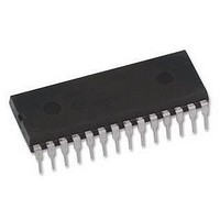
IR21365C International Rectifier, IR21365C Datasheet - Page 2

IR21365C
Manufacturer Part Number
IR21365C
Description
IC, MOSFET DRIVER, HALF BRIDGE, DIP-28
Manufacturer
International Rectifier
Datasheet
1.IR21362JTRPBF.pdf
(36 pages)
Specifications of IR21365C
Device Type
Half Bridge
Peak Output Current
350mA
Output Resistance
50ohm
Input Delay
425ns
Output Delay
400ns
Supply Voltage Range
12V To 20V
Driver Case Style
DIP
No. Of Pins
28
Lead Free Status / RoHS Status
na
Absolute Maximum Ratings
Absolute Maximum Ratings indicate sustained limits beyond which damage to the device may occur. All voltage
parameters are absolute voltages referenced to COM. The thermal resistance and power dissipation ratings are
measured under board mounted and still air conditions.
Recommended Operating Conditions
The input/output logic-timing diagram is shown in Fig. 1. For proper operation the device should be used within the
recommended conditions. All voltage parameters are absolute referenced to COM. The V
with all supplies biased at a 15 V differential.
Note 1: Logic operational for V
Note 2: All input pins and the ITRIP and EN pins are internally clamped with a 5.2 V zener diode.
www.irf.com
Symbol
Symbol
V
V
V
V
V
V
dV/dt
Rth
V
HO 1,2,3
V
V
LO1,2,3
LO1,2,3
V
V
V
(Please refer to the Design Tip DT97-3 for more details).
V
S 1,2,3
V
V
B1,2,3
V
V
P
RCIN
T
T
T
RCIN
FLT
FLT
HO
CC
CC
SS
SS
IN
S
B
D
S
J
L
JA
High side offset voltage
High side floating supply voltage
High side floating output voltage
Low side and logic fixed supply voltage
Logic ground
Low side output voltage
Input voltage LIN, HIN, ITRIP, EN
RCIN input voltage
FAULT output voltage
Allowable offset voltage slew rate
Package power dissipation
@ T
Thermal resistance, junction to
ambient
Junction temperature
Storage temperature
Lead temperature (soldering, 10 seconds)
High side floating supply voltage
High side floating supply offset voltage
High side output voltage
Low side output voltage
Low side and logic fixed supply
voltage
Logic ground
FAULT output voltage
RCIN input voltage
A
S
≤ +25 °C
of (COM - 5 V) to (COM + 600 V). Logic state held for V
Definition
Definition
IR213(6,62,63,65,66,67,68)(J&S) & PbF
IR213(6,68)
IR21362
IR213(6,63,65,66,67)
IR213(6,68)
IR21362
IR213(6,63,65,66,67) V
(28 lead PDIP)
(28 lead SOIC)
(44 lead PLCC)
(28 lead PDIP)
(28 lead SOIC)
(44 lead PLCC)
V
V
V
V
S1,2,3
V
V
V
S1,2,3
V
B 1,2,3
S1,2,3
S1,2,3
Note 1
V
CC
SS
SS
SS
Min
Min
11.5
-0.3
-0.3
-0.3
V
V
-55
S1,2,3
10
12
—
—
—
—
—
—
—
—
—
-5
0
SS
SS
S
-0.3
-0.3
-0.3
- 25
+11.5
- 0.3 V
+10
+12
- 25 V
of (COM - 5 V) to (COM – V
S
offset ratings are tested
(V
V
V
V
V
V
V
V
V
B 1,2,3
B 1,2,3
Lower of
SS
CC
S1,2,3
S1,2,3
S1,2,3
CC
CC
CC
CC
Max
V
Max
625
150
150
300
1.5
1.6
2.0
+ 15) or
600
25
50
83
78
63
V
V
V
B1,2,3
+ 0.3)
20
20
20
+ 0.3
+ 0.3
+ 0.3
+ 0.3
5
CC
CC
CC
+ 0.3
+ 0.3
+ 20
+ 20
+ 20
Units
°C/W
V/ns
Units
°C
W
V
V
BS
).
2


