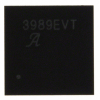
A3989SEVTR-T Allegro Microsystems Inc, A3989SEVTR-T Datasheet - Page 5

A3989SEVTR-T
Manufacturer Part Number
A3989SEVTR-T
Description
IC, MOTOR DRIVER, STEPPER, 1.2A, QFN-36
Manufacturer
Allegro Microsystems Inc
Datasheet
1.A3989SEVTR-T.pdf
(12 pages)
Specifications of A3989SEVTR-T
Motor Type
Stepper
No. Of Outputs
3
Output Current
1.2A
Output Voltage
36V
Supply Voltage Range
3V To 5.5V
Driver Case Style
QFN
No. Of Pins
36
Applications
DC Motor Driver, Stepper Motor Driver
Number Of Outputs
2
Voltage - Load
8 V ~ 36 V
Voltage - Supply
3 V ~ 5.5 V
Operating Temperature
-20°C ~ 85°C
Mounting Type
Surface Mount
Package / Case
36-VFQFN Exposed Pad
Rohs Compliant
Yes
Lead Free Status / RoHS Status
Lead free / RoHS Compliant
Current - Output
-
Lead Free Status / RoHS Status
Lead free / RoHS Compliant, Lead free / RoHS Compliant
Other names
620-1183-2
A3989
Device Operation
dc motor and one bipolar stepper motor. The currents in each of
the full bridges, all N-channel DMOS, are regulated with fixed
off-time pulse width modulated (PWM) control circuitry. The
peak current in each full bridge is set by the value of an external
current sense resistor, R
If the logic inputs are pulled up to VDD, it is good practice to use
a high value pullup resistor in order to limit current to the logic
inputs should an overvoltage event occur. Logic inputs include:
PHASEx, I0x, I1x, ENABLE, and MODE.
Internal PWM Current Control
controlled by a fixed off-time PWM current control circuit that
limits the load current to a user-specified value, I
a diagonal pair of source and sink DMOS outputs are enabled
and current flows through the motor winding and R
voltage across the current sense resistor equals the voltage on the
VREFx pin, the current sense comparator resets the PWM latch,
which turns off the source driver.
The maximum value of current limiting is set by the selection of
R
function approximated by:
The stepper motor outputs will define each current step as a
percentage of the maximum current, I
each step I
where % I
Note: It is critical to ensure that the maximum rating of 500 mV
on each SENSEx pin is not exceeded.
Fixed Off-Time
uses a one shot circuit to control the time the drivers remain off.
The one shot off-time, t
S
and the voltage at the VREF input with a transconductance
TripMax
Trip
is approximated by:
I
is given in the Step Sequencing table.
Trip
The internal PWM current control circuitry
I
= (% I
TripMax
The A3989 is designed to operate one
off
Sx
, is internally set to 30 μs.
, and a reference voltage, V
TripMax
= V
REF
Bipolar Stepper and High Current DC Motor Driver
/ 100) I
/ (3×R
TripMax
Each full-bridge is
TripMax
S
)
. The actual current at
TRIP
Functional Description
Functional Description
Sx
. Initially,
. When the
REFx
.
Blanking
comparator when the outputs are switched by the internal current
control circuitry. The comparator output is blanked to prevent
false detections of overcurrent conditions, due to reverse recovery
currents of the clamp diodes, or to switching transients related to
the capacitance of the load. Dc motors require more blank time
than stepper motors. The stepper driver blank time, t
is approximately 1 s. The dc driver blank time, t
approximately 3 s.
Control Logic
via industry standard I1, I0, and PHASE interface. This commu-
nication logic allows for full, half, and quarter step modes. Each
bridge also has an independent V
modes can be programmed by dynamically changing the voltage
on the corresponding VREFx pin. The dc motor is controlled using
standard PHASE, ENABLE communication. Fast or slow current
decay during the off-time is selected via the MODE pin.
Charge Pump (CP1 and CP2)
generate a gate supply greater than the V
source-side DMOS gates. A 0.1 F ceramic capacitor should be
connected between CP1 and CP2 for pumping purposes. A 0.1 F
ceramic capacitor is required between VCP and VBBx to act as a
reservoir to operate the high-side DMOS devices.
Shutdown
perature, or low voltage on VCP), the outputs of the device are
disabled until the fault condition is removed. At power-up, the
undervoltage lockout (UVLO) circuit disables the drivers.
Synchronous Rectification
triggered by an internal fixed off-time cycle, load current will
recirculate. The A3989 synchronous rectification feature will
turn on the appropriate MOSFETs during the current decay. This
effectively shorts the body diode with the low R
significantly lowers power dissipation. When a zero current level
This function blanks the output of the current sense
In the event of a fault (excessive junction tem-
Stepper motor communication is implemented
115 Northeast Cutoff
1.508.853.5000; www.allegromicro.com
Allegro MicroSystems, Inc.
Worcester, Massachusetts 01615-0036 U.S.A.
REF
When a PWM-off cycle is
input so higher resolution step
The charge pump is used to
BB
in order to drive the
DS(on)
BLANKdc
BLANKst
driver. This
, is
,
5


