74LVC132AD NXP Semiconductors, 74LVC132AD Datasheet
74LVC132AD
Specifications of 74LVC132AD


Related parts for 74LVC132AD


74LVC132AD Summary of contents
Page 1
Quad 2-input NAND Schmitt trigger Rev. 01 — 15 December 2006 1. General description The 74LVC132A is a high-performance, low-power, low-voltage, Si-gate CMOS device, superior to most advanced CMOS compatible TTL families. The 74LVC132A provides four 2-input NAND gates ...
Page 2
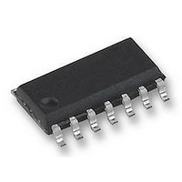
... NXP Semiconductors 4. Ordering information Table 1. Ordering information Type number Package Temperature range Name 74LVC132AD +125 C 74LVC132APW +125 C 74LVC132ABQ +125 C 5. Functional diagram mna212 Fig 1. Logic symbol 74LVC132A_1 Product data sheet Description SO14 plastic small outline package; 14 leads; body width 3.9 mm TSSOP14 plastic thin shrink small outline package ...
Page 3
... NXP Semiconductors 6. Pinning information 6.1 Pinning 74LVC132A GND Fig 4. Pin configuration SO14 and TSSOP14 6.2 Pin description Table 2. Pin description Symbol Pin GND 74LVC132A_1 Product data sheet 001aaf590 (1) The die substrate is attached to this pad using Fig 5. Pin configuration DHVQFN14 ...
Page 4
... NXP Semiconductors 7. Functional description [1] Table 3. Function table Input [ HIGH voltage level LOW voltage level. 8. Limiting values Table 4. Limiting values In accordance with the Absolute Maximum Rating System (IEC 60134). Voltages are referenced to GND (ground = 0 V). Symbol Parameter V supply voltage CC V input voltage ...
Page 5
... NXP Semiconductors 10. Static characteristics Table 6. Static characteristics At recommended operating conditions. Voltages are referenced to GND (ground = 0 V). Symbol Parameter +85 C amb V HIGH-level output voltage OH V LOW-level output voltage OL I input leakage current I I supply current CC I additional supply current CC C input capacitance ...
Page 6
... NXP Semiconductors 11. Dynamic characteristics Table 7. Dynamic characteristics Voltages are referenced to GND (ground = 0 V). For test circuit see Symbol Parameter t propagation delay pd t output skew time sk(o) C power dissipation PD capacitance [1] Typical values are measured the same as t and PLH PHL [3] Skew between any two outputs of the same package switching in the same direction. This parameter is guaranteed by design. ...
Page 7
... NXP Semiconductors Test data is given in Table 8. Definitions for test circuit Load resistance Load capacitance including jig and probe capacitance Termination resistance should be equal to output impedance External voltage for measuring switching times. EXT Fig 7. Load circuitry for switching times Table 8. Test data ...
Page 8
... NXP Semiconductors 13. Transfer characteristics Table 9. Transfer characteristics Voltages are referenced to GND (ground = 0 V); for test circuit see Symbol Parameter Conditions V positive-going see T+ threshold voltage V negative-going see T threshold voltage V hysteresis voltage (V H Figure 9 74LVC132A_1 Product data sheet Figure Figure 8 and Figure 1.2 V ...
Page 9
... NXP Semiconductors 14. Waveforms transfer characteristics Fig 8. Transfer characteristic Fig 10. Typical transfer characteristic; V 74LVC132A_1 Product data sheet mna207 Fig 9. Definition (mA 0.6 1.2 1 Rev. 01 — 15 December 2006 74LVC132A Quad 2-input NAND Schmitt trigger and mna582 2 (V) I © NXP B.V. 2006. All rights reserved. ...
Page 10
... NXP Semiconductors 15. Package outline SO14: plastic small outline package; 14 leads; body width 3 pin 1 index 1 e DIMENSIONS (inch dimensions are derived from the original mm dimensions) A UNIT max. 0.25 1.45 mm 1.75 0.25 0.10 1.25 0.010 0.057 inches 0.01 0.069 0.004 0.049 Note 1. Plastic or metal protrusions of 0.15 mm (0.006 inch) maximum per side are not included. ...
Page 11
... NXP Semiconductors TSSOP14: plastic thin shrink small outline package; 14 leads; body width 4 pin 1 index 1 e DIMENSIONS (mm are the original dimensions) A UNIT max. 0.15 0.95 mm 1.1 0.25 0.05 0.80 Notes 1. Plastic or metal protrusions of 0.15 mm maximum per side are not included. 2. Plastic interlead protrusions of 0.25 mm maximum per side are not included. ...
Page 12
... NXP Semiconductors DHVQFN14: plastic dual in-line compatible thermal enhanced very thin quad flat package; no leads; 14 terminals; body 2 0.85 mm terminal 1 index area terminal 1 index area DIMENSIONS (mm are the original dimensions) (1) A UNIT max. 0.05 0. 0.2 0.00 0.18 Note 1. Plastic or metal protrusions of 0.075 mm maximum per side are not included. ...
Page 13
... NXP Semiconductors 16. Abbreviations Table 10. Abbreviations Acronym Description CDM Charged Device Model CMOS Complementary Metal Oxide Semiconductor DUT Device Under Test ESD ElectroStatic Discharge HBM Human Body Model MM Machine Model TTL Transistor-Transistor Logic 17. Revision history Table 11. Revision history Document ID Release date 74LVC132A_1 ...
Page 14
... For detailed and full information see the relevant full data sheet, which is available on request via the local NXP Semiconductors sales office. In case of any inconsistency or conflict with the short data sheet, the full data sheet shall prevail ...
Page 15
... NXP Semiconductors 20. Contents 1 General description . . . . . . . . . . . . . . . . . . . . . . 1 2 Features . . . . . . . . . . . . . . . . . . . . . . . . . . . . . . . 1 3 Applications . . . . . . . . . . . . . . . . . . . . . . . . . . . . 1 4 Ordering information . . . . . . . . . . . . . . . . . . . . . 2 5 Functional diagram . . . . . . . . . . . . . . . . . . . . . . 2 6 Pinning information . . . . . . . . . . . . . . . . . . . . . . 3 6.1 Pinning . . . . . . . . . . . . . . . . . . . . . . . . . . . . . . . 3 6.2 Pin description . . . . . . . . . . . . . . . . . . . . . . . . . 3 7 Functional description . . . . . . . . . . . . . . . . . . . 4 8 Limiting values Recommended operating conditions Static characteristics Dynamic characteristics . . . . . . . . . . . . . . . . . . 6 12 Waveforms . . . . . . . . . . . . . . . . . . . . . . . . . . . . . 6 13 Transfer characteristics Waveforms transfer characteristics ...