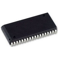
AS7C4096A-12JIN ALLIANCE MEMORY, AS7C4096A-12JIN Datasheet

AS7C4096A-12JIN
Specifications of AS7C4096A-12JIN
Related parts for AS7C4096A-12JIN
AS7C4096A-12JIN Summary of contents
Page 1
... SOJ - 44-pin TSOP 2 • ESD protection ≥ 2000 volts • Latch-up current ≥ 200 mA Pin arrangement 36-pin SOJ (400 mil I/O1 7 I/ GND 10 I/ Control OE Circuit CE – 160 10 Alliance Semiconductor AS7C4096A s 44-pin TSOP A18 A17 A16 A15 I/ I/O7 I/ GND I/ ...
Page 2
... Functional description The AS7C4096A is a high-performance CMOS 4,194,304-bit Static Random Access Memory (SRAM) device organized as 524,288 words × 8 bits designed for memory applications where fast data access, low power, and simple interfacing are desired. Equal address access and cycle times (t for high-performance applications. The chip enable input CE permits easy memory expansion with multiple-bank memory systems ...
Page 3
... V – 0.2V – mA Min CC – mA Min CC 2.4 = –4 mA Min NOMINAL) CC Symbol Signals C A, CE, WE I/O I/O Alliance Semiconductor AS7C4096A Min Nominal Max 4.5 5.0 5.5 2.2 – –0.5 – 0.8 0 – 70 –40 – 85 –12 –15 –20 1 – 1 – 1 – – ...
Page 4
... OLZ t – 5 – OHZ t 0 – – 10 – Falling input 2,5,6 Data valid 2,5,7,8 t RC1 OLZ Data valid 50% Alliance Semiconductor AS7C4096A –15 –20 Min Max Min Max – 15 – 20 – – 15 – 20 – 15 – – 6 – 6 – 3 – 3 – – 3 – 3 – ...
Page 5
... – 0 – – 6 – – 0 – – 3 – Data valid t WZ Alliance Semiconductor AS7C4096A –15 –20 Min Max Min Max Unit Notes 15 – 20 – – 12 – – 12 – – 0 – – 12 – – 20 – – 0 – – 0 – – ...
Page 6
... All write cycle timings are referenced from the last valid address to the first transitioning address 30pF, except at high Z and low Z parameters, where C = 5pF. 2/21/06, v 1.2 ® Data valid +5.0V 480Ω D OUT 10 255Ω C GND Figure B: 5.0V Output load required to meet I specification Alliance Semiconductor AS7C4096A t DH Thevenin equivalent: 168Ω +1.728V D OUT ...
Page 7
... 36-pin SOJ Pin 1 A2 2/21/06, v 1.2 ® 2726 1819 0–5° Seating b Plane c E Alliance Semiconductor AS7C4096A c 44-pin TSOP 2 Min(mm) Max( 0.30 c 0.12 d 18.31 18.52 E 10.06 10. 11. 0.80 (typical) L 0.40 36-pin SOJ 400 Min(mils) Max(mils) A 0.128 A 0.025 1 A 0.105 ...
Page 8
... Version Commercial AS7C4096A-10JC SOJ Industrial AS7C4096A-10JI Commercial AS7C4096A-10TC TSOP 2 Industrial AS7C4096A-10TI Note: Add suffix ‘N’ to the above part number for Lead Free Parts. (Ex: AS7C4096A - 10 TIN) Part numbering system AS7C 4096A –XX SRAM Device Access time prefix number 2/21/06, v 1.2 ® ...
Page 9
... Revision History Rev. No. v1.0 Initial release Included & SB1 v1.1 Corrected the following: T v1.2 Removed the title ”PRELIMINARY INFORMATION” 2/21/06, v 1.2 ® History parameters , V V & IH Alliance Semiconductor AS7C4096A Revised Date 11/08/04 05/27/05 02/21/ ...
Page 10
... Alliance products in such life- supporting systems implies that the manufacturer assumes all risk of such use and agrees to indemnify Alliance against all claims arising from such use. ® Copyright © Alliance Semiconductor All Rights Reserved Part Number: AS7C4096A Document Version: v 1.2 AS7C4096A ...


