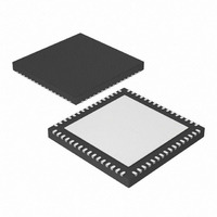
PIC24FJ192GA106-I/MR Microchip Technology, PIC24FJ192GA106-I/MR Datasheet - Page 9

PIC24FJ192GA106-I/MR
Manufacturer Part Number
PIC24FJ192GA106-I/MR
Description
IC, 16BIT MCU, PIC24F, 32MHZ, QFN-64
Manufacturer
Microchip Technology
Series
PIC® 24Fr
Datasheets
1.PIC24FJ128GA008-IPT.pdf
(12 pages)
2.PIC24FJ128GA106-IPT.pdf
(14 pages)
3.PIC24FJ128GA106-IPT.pdf
(330 pages)
4.PIC24FJ128GA106-IPT.pdf
(52 pages)
5.PIC24FJ128GB110-IPF.pdf
(292 pages)
Specifications of PIC24FJ192GA106-I/MR
Controller Family/series
PIC24
No. Of I/o's
53
Ram Memory Size
16KB
Cpu Speed
32MHz
No. Of Timers
5
Core Size
16 Bit
Program Memory Size
192KB
Peripherals
ADC, Comparator, PWM, RTC, Timer
Core Processor
PIC
Speed
32MHz
Connectivity
I²C, PMP, SPI, UART/USART
Number Of I /o
53
Program Memory Type
FLASH
Ram Size
16K x 8
Voltage - Supply (vcc/vdd)
2 V ~ 3.6 V
Data Converters
A/D 16x10b
Oscillator Type
Internal
Operating Temperature
-40°C ~ 85°C
Package / Case
64-VFQFN, Exposed Pad
Processor Series
PIC24FJ
Core
PIC
Data Bus Width
16 bit
Data Ram Size
16 KB
Interface Type
I2C, SPI, UART
Maximum Clock Frequency
32 MHz
Number Of Programmable I/os
53
Number Of Timers
5
Maximum Operating Temperature
+ 85 C
Mounting Style
SMD/SMT
3rd Party Development Tools
52713-733, 52714-737, 53276-922, EWDSPIC
Development Tools By Supplier
PG164130, DV164035, DV244005, DV164005, PG164120, DM240011, DM240001
Minimum Operating Temperature
- 40 C
On-chip Adc
10 bit, 16 Channel
Lead Free Status / RoHS Status
Lead free / RoHS Compliant
For Use With
876-1004 - PIC24 BREAKOUT BOARD
Eeprom Size
-
Lead Free Status / Rohs Status
Details
9. Module: 10-Bit High-Speed A/D
REGISTER 20-1:
© 2009 Microchip Technology Inc.
bit 7-5
In Register 20-1 (AD1CON1), the descriptions
provided for the various combinations of the
SSRC<2:0> bits (ADCON1<7:5>) are incorrect.
Specifically, while the number and type of trigger
sources are reported correctly, several are
associated with the wrong bit combinations.
The correct order of trigger sources is listed below
(changes in bold).
Converter
SSRC2:SSRC0: Conversion Trigger Source Select bits
111 = Internal counter ends sampling and starts conversion (auto-convert)
110 = CTMU event ends sampling and starts conversion
101 = Reserved
100 = Timer5 compare ends sampling and starts conversion
011 = Reserved
010 = Timer3 compare ends sampling and starts conversion
001 = Active transition on INT0 pin ends sampling and starts conversion
000 = Clearing SAMP bit ends sampling and starts conversion
AD1CON1: A/D CONTROL REGISTER 1 (PARTIAL REPRESENTATION)
PIC24FJ256GA110 FAMILY
10. Module: Special Features
In Register 24-3 (CW3), the explanatory text with
Configuration bits, WPFP<8:0> (CW3<8:0>), is
changed to agree with the text of Section 24.4.2
“Code Segment Protection”. The new register
text is as follows (change in bold):
“Designates the 512-byte program code page that
is the boundary of the protected code segment,
starting with Page 0 at the bottom of program
memory.”
DS80385B-page 9


