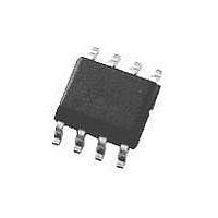
LM2662M National Semiconductor, LM2662M Datasheet - Page 7

LM2662M
Manufacturer Part Number
LM2662M
Description
IC, DC/DC VOLTAGE CONVERTER, 8-SOIC
Manufacturer
National Semiconductor
Datasheet
1.LM2662M.pdf
(14 pages)
Specifications of LM2662M
Primary Input Voltage
5V
No. Of Outputs
1
Output Current
200mA
No. Of Pins
8
Operating Temperature Range
-40°C To +85°C
Power Dissipation Pd
735mW
Supply Voltage Range
1.5V To 5.5V
Lead Free Status / RoHS Status
Contains lead / RoHS non-compliant
Available stocks
Company
Part Number
Manufacturer
Quantity
Price
Part Number:
LM2662M
Manufacturer:
NS/国半
Quantity:
20 000
Part Number:
LM2662MX
Manufacturer:
TI/德州仪器
Quantity:
20 000
Company:
Part Number:
LM2662MX/NOPB
Manufacturer:
TI
Quantity:
42
Part Number:
LM2662MX/NOPB
Manufacturer:
NS/国半
Quantity:
20 000
Application Information
SIMPLE NEGATIVE VOLTAGE CONVERTER
The main application of LM2662/LM2663 is to generate a
negative supply voltage. The voltage inverter circuit uses only
two external capacitors as shown in the Basic Application
Circuits. The range of the input supply voltage is 1.5V to 5.5V.
For a supply voltage less than 3.5V, the LV pin must be con-
nected to ground to bypass the internal regulator circuitry.
This gives the best performance in low voltage applications.
If the supply voltage is greater than 3.5V, LV may be con-
nected to ground or left open. The choice of leaving LV open
simplifies the direct substitution of the LM2662/LM2663 for
the LMC7660 Switched Capacitor Voltage Converter.
The output characteristics of this circuit can be approximated
by an ideal voltage source in series with a resistor. The volt-
age source equals −(V+). The output resistance R
function of the ON resistance of the internal MOS switches,
the oscillator frequency, and the capacitance and ESR of C
and C
C
the ESR of the pumping capacitor C
the output resistance. The output capacitor C
discharging at a current approximately equal to the output
current, therefore, its ESR only counts once in the output re-
sistance. A good approximation is:
where R
MOS switches shown in Figure 2.
High value, low ESR capacitors will reduce the output resis-
tance. Instead of increasing the capacitance, the oscillator
frequency can be increased to reduce the 2/(f
Once this term is trivial compared with R
increasing in oscillator frequency and capacitance will be-
come ineffective.
The peak-to-peak output voltage ripple is determined by the
oscillator frequency, and the capacitance and ESR of the out-
put capacitor C
Again, using a low ESR capacitor will result in lower ripple.
POSITIVE VOLTAGE DOUBLER
The LM2662/LM2663 can operate as a positive voltage dou-
bler (as shown in the Basic Application Circuits). The doubling
function is achieved by reversing some of the connections to
1
is approximately twice as the output current, the effect of
2
. Since the switching current charging and discharging
SW
FIGURE 2. Voltage Inverting Principle
is the sum of the ON resistance of the internal
2
:
1
is multiplied by four in
SW
and ESRs, further
2
is charging and
osc
× C
1
out
) term.
10000322
is a
1
7
the device. The input voltage is applied to the GND pin with
an allowable voltage from 2.5V to 5.5V. The V+ pin is used
as the output. The LV pin and OUT pin must be connected to
ground. The OSC pin can not be driven by an external clock
in this operation mode. The unloaded output voltage is twice
of the input voltage and is not reduced by the diode D
ward drop.
The Schottky diode D
oscillator circuit uses the V+ pin and the LV pin (connected to
ground in the voltage doubler circuit) as its power rails. Volt-
age across V+ and LV must be larger than 1.5V to insure the
operation of the oscillator. During start-up, D
charge up the voltage at V+ pin to start the oscillator; also, it
protects the device from turning-on its own parasitic diode and
potentially latching-up. Therefore, the Schottky diode D
should have enough current carrying capability to charge the
output capacitor at start-up, as well as a low forward voltage
to prevent the internal parasitic diode from turning-on. A
Schottky diode like 1N5817 can be used for most applica-
tions. If the input voltage ramp is less than 10V/ms, a smaller
Schottky diode like MBR0520LT1 can be used to reduce the
circuit size.
SPLIT V+ IN HALF
Another interesting application shown in the Basic Application
Circuits is using the LM2662/LM2663 as a precision voltage
divider. Since the off-voltage across each switch equals V
2, the input voltage can be raised to +11V.
CHANGING OSCILLATOR FREQUENCY
For the LM2662, the internal oscillator frequency can be se-
lected using the Frequency Control (FC) pin. When FC is
open, the oscillator frequency is 20 kHz; when FC is connect-
ed to V+, the frequency increases to 150 kHz. A higher
oscillator frequency allows smaller capacitors to be used for
equivalent output resistance and ripple, but increases the typ-
ical supply current from 0.3 mA to 1.3 mA.
The oscillator frequency can be lowered by adding an external
capacitor between OSC and GND (See typical performance
characteristics). Also, in the inverter mode, an external clock
that swings within 100 mV of V+ and GND can be used to
drive OSC. Any CMOS logic gate is suitable for driving OSC.
LV must be grounded when driving OSC. The maximum ex-
ternal clock frequency is limited to 150 kHz.
The switching frequency of the converter (also called the
charge pump frequency) is half of the oscillator frequency.
Note: OSC cannot be driven by an external clock in the voltage-doubling
Open
V+
Open or V+
N/A
TABLE 1. LM2662 Oscillator Frequency Selection
mode.
FC
Open
Open
External Capacitor
External Clock
(inverter mode only)
1
is only needed for start-up. The internal
OSC
20 kHz
150 kHz
See Typical
Performance
Characteristics
External Clock
Frequency
Oscillator
1
www.national.com
is used to
1
's for-
IN
1
/


