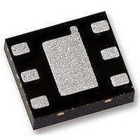
LP5900SD-2.2 National Semiconductor, LP5900SD-2.2 Datasheet

LP5900SD-2.2
Specifications of LP5900SD-2.2
Related parts for LP5900SD-2.2
LP5900SD-2.2 Summary of contents
Page 1
... No Noise Bypass Capacitor Required ■ Logic Controlled Enable ■ Thermal-overload and short-circuit protection ■ −40°C to +125°C junction temperature range for operation Typical Application Circuit © 2008 National Semiconductor Corporation Key Specifications ■ Input voltage range ■ Output voltage range ■ Output current ■ ...
Page 2
Connection Diagrams The actual physical placement of the package marking will vary from part to part. Pin Descriptions Pin No. micro SMD LLP Pad www.national.com 4-Bump Thin micro SMD Package, Large Bump ...
Page 3
... For availability contact National Semiconductor local sales office For LLP-6 Package Output Voltage (V) 250 Units Tape and Reel 1.5 LP5900SD-1.5/NOPB 1.8 LP5900SD-1.8/NOPB 2.0 LP5900SD-2.0/NOPB 2.2 LP5900SD-2.2/NOPB 2.5 LP5900SD-2.5/NOPB 2.7 LP5900SD-2.7/NOPB 2.8 LP5900SD-2.8/NOPB 3.0 LP5900SD-3.0/NOPB 3.3 LP5900SD-3.3/NOPB Supplied As 3k Units Tape and Reel LP5900TLX-1 ...
Page 4
... Absolute Maximum Ratings If Military/Aerospace specified devices are required, please contact the National Semiconductor Sales Office/ Distributors for availability and specifications. V Pin: Input Voltage IN V Pin: Output Voltage -0 OUT V Pin: Enable Input Voltage -0 Continuous Power Dissipation (Note 3) Junction Temperature (T ) JMAX Storage Temperature Range Maximum Lead Temperature (Soldering, 10 sec ...
Page 5
Symbol Parameter Login Input Thresholds V Low Input Threshold ( High Input Threshold ( Input Current at V Pin EN EN (Note 14) Transient Characteristics ΔV Line Transient OUT (Note 15) Load Transient (Note ...
Page 6
Typical Performance Characteristics. + 1.0V 1.2V 1mA , T (NOM) EN OUT Output Noise Density Power Supply Rejection Ratio Ground Current vs V www.national.com Unless otherwise specified,C = 25ºC. A 20144157 20144159 I = 0mA IN, ...
Page 7
Ground Current 100mA IN, LOAD 20144153 Short Circuit Current 20144148 Line Transient 20144155 Ground Current vs Load Current Load Transient Enable Start-up Time 1mA 20144150 20144149 = 2.8V) OUT 20144144 www.national.com ...
Page 8
Enable Start-up Time 100mA Enable Start-up Time 100mA Application Hints POWER DISSIPATION AND DEVICE OPERATION The permissible power dissipation for any package is a mea- sure of the capability of the device ...
Page 9
... Electrical Characteristics section under V micro SMD MOUNTING The micro SMD package requires specific mounting tech- niques, which are detailed in National Semiconductor Appli- cation Note AN-1112. For best results during assembly, alignment ordinals on the PC board may be used to facilitate placement of the micro SMD device ...
Page 10
Physical Dimensions www.national.com inches (millimeters) unless otherwise noted 4-Bump Thin micro SMD NS Package Number TLA04CDA The dimensions for X1, X2 and X3 are given as 1.065 mm ± 0.030 1.090 mm ± 0.030 mm ...
Page 11
Notes 11 www.national.com ...
Page 12
... For more National Semiconductor product information and proven design tools, visit the following Web sites at: Products Amplifiers www.national.com/amplifiers Audio www.national.com/audio Clock Conditioners www.national.com/timing Data Converters www.national.com/adc Displays www.national.com/displays Ethernet www.national.com/ethernet Interface www.national.com/interface LVDS www.national.com/lvds Power Management www.national.com/power Switching Regulators www.national.com/switchers LDOs www ...


