AD8592ARMZ Analog Devices Inc, AD8592ARMZ Datasheet
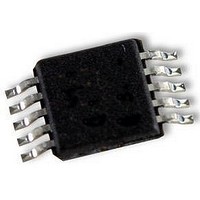
OP AMP, +SHUTDOWN RRI/O, SMD, 8592

AD8592ARMZ

Manufacturer Part Number
AD8592ARMZ
Description
OP AMP, +SHUTDOWN RRI/O, SMD, 8592
Manufacturer
Analog Devices Inc
Datasheet

Specifications of AD8592ARMZ

Op Amp Type
Low Input Bias
No. Of Amplifiers
2
Bandwidth
2.2MHz
Slew Rate
5V/µs
Supply Voltage Range
2.5V To 6V
Amplifier Case Style
MSOP
No. Of Pins
10
Operating Temperature Range
-40°C To
Lead Free Status / RoHS Status
Lead free / RoHS Compliant

Available stocks

Company
Part Number
Manufacturer
Quantity
Price
Part Number:
AD8592ARMZ
Manufacturer:
Analog Devices Inc
Quantity:
31 712
Part Number:
AD8592ARMZ
Manufacturer:
AD
Quantity:
8 241
Part Number:
AD8592ARMZ
Manufacturer:
ADI/亚德诺
Quantity:
20 000
Part Number:
AD8592ARMZ-REEL
Manufacturer:
AD
Quantity:
1 538
Part Number:
AD8592ARMZ-REEL
Manufacturer:
Microsemi
Quantity:
1 538
Part Number:
AD8592ARMZ-REEL
Manufacturer:
ADI/PBF
Quantity:
14 813
Part Number:
AD8592ARMZ-REEL
Manufacturer:
ADI/亚德诺
Quantity:
20 000
Part Number:
AD8592ARMZ-REEL7
Manufacturer:
TOREX
Quantity:
800
a
GENERAL DESCRIPTION
The AD8591, AD8592 and AD8594 are single, dual and quad
rail-to-rail input and output single supply amplifiers featuring
250 mA output drive current and a power saving shutdown
mode. The AD8592 includes an independent shutdown func-
tion for each amplifier. When both amplifiers are in shutdown
mode the total supply current is reduced to less than 1 A. The
AD8591 and AD8594 include a single master shutdown func-
tion that reduces total supply current to less than 1 A. All
amplifier outputs are in a high impedance state when in shut-
down mode.
These amplifiers have very low input bias currents, making them
suitable for integrators and diode amplification. Outputs are
stable with virtually any capacitive load. Supply current is less
than 750 A per amplifier in active mode.
Applications for these amplifiers include audio amplification for
portable computers, portable phone headsets, sound ports, sound
cards and set-top boxes. The AD859x family is capable of driving
heavy capacitive loads such as LCD panel reference levels.
The ability to swing rail-to-rail at both the input and output
enables designers to buffer CMOS DACs, ASICs and other
wide output swing devices in single supply systems.
The AD8591, AD8592 and AD8594 are specified over the indus-
trial (–40 C to +85 C) temperature range. The AD8591, single,
is available in the tiny 6-lead SOT package. The AD8592, dual, is
available in the 10-lead SOIC surface mount package. The
AD8594, quad, is available in 16-lead narrow SOIC and 16-lead
TSSOP packages.
REV. A
Information furnished by Analog Devices is believed to be accurate and
reliable. However, no responsibility is assumed by Analog Devices for its
use, nor for any infringements of patents or other rights of third parties
which may result from its use. No license is granted by implication or
otherwise under any patent or patent rights of Analog Devices.
FEATURES
Single Supply Operation: +2.5 V to +6 V
High Output Current:
Extremely Low Shutdown Supply Current: 100 nA
Low Supply Current: 750 A/Amp
Wide Bandwidth: 3 MHz
Slew Rate: 5 V/ s
No Phase Reversal
Very Low Input Bias Current
High Impedance Outputs When in Shutdown Mode
Unity Gain Stable
APPLICATIONS
Mobile Communication Handset Audio
PC Audio
PCMCIA/Modem Line Driving
Battery Powered Instrumentation
Data Acquisition
ASIC Input or Output Amplifier
LCD Display Reference Level Driver
250 mA
Operational Amplifiers with Shutdown
One Technology Way, P.O. Box 9106, Norwood, MA 02062-9106, U.S.A.
Tel: 781/329-4700
Fax: 781/326-8703
AD8591/AD8592/AD8594
Rail-to-Rail Input/Output
OUT A
OUT B
OUT A
PIN CONFIGURATIONS
OUT A
OUT A
OUT B
–IN A
+IN A
SDA
IN A
IN A
IN B
IN B
IN A
16-Lead Narrow SOIC
World Wide Web Site: http://www.analog.com
IN A
IN A
IN B
IN B
V
V
NC
V–
V
NC
16-Lead TSSOP
10-Lead SOIC
NC = NO CONNECT
CMOS Single Supply
1
2
3
4
5
6
7
8
NC = NO CONNECT
1
2
3
1
2
3
4
5
6-Lead SOT
(RM Suffix)
(RU Suffix)
(RT Suffix)
(Not to Scale)
(Not to Scale)
(R Suffix)
AD8594
TOP VIEW
1
1
8
AD8591
AD8594
AD8592
16
9
16
15
14
13
12
11
10
9
10
6
5 SD
4
9
8 –IN B
7
6
© Analog Devices, Inc., 1999
OUT D
V
OUT C
SD
OUT D
V
+IN C
OUT C
SD
V
V+
OUT B
+IN B
SDB
IN D
IN D
IN C
IN C
IN D
IN D
IN C
IN A

Related parts for AD8592ARMZ

AD8592ARMZ Summary of contents

Page 1

FEATURES Single Supply Operation: +2 High Output Current: 250 mA Extremely Low Shutdown Supply Current: 100 nA Low Supply Current: 750 A/Amp Wide Bandwidth: 3 MHz Slew Rate Phase Reversal Very ...

Page 2

AD8591/AD8592/AD8594–SPECIFICATIONS ELECTRICAL CHARACTERISTICS Parameter INPUT CHARACTERISTICS Offset Voltage Input Bias Current Input Offset Current Input Voltage Range Common-Mode Rejection Ratio Large Signal Voltage Gain Offset Voltage Drift Bias Current Drift Offset Current Drift OUTPUT CHARACTERISTICS Output Voltage High Output Voltage ...

Page 3

ELECTRICAL CHARACTERISTICS Parameter INPUT CHARACTERISTICS Offset Voltage Input Bias Current Input Offset Current Input Voltage Range Common-Mode Rejection Ratio Large Signal Voltage Gain Offset Voltage Drift Bias Current Drift Offset Current Drift OUTPUT CHARACTERISTICS Output Voltage High Output Voltage Low ...

Page 4

AD8591/AD8592/AD8594 ABSOLUTE MAXIMUM RATINGS Supply Voltage . . . . . . . . . . . . . . . . . . . . . . . . . . . . . . . . . +6 ...

Page 5

0.7 0.6 0.5 0.4 0.3 0.2 0.1 0 0.75 1.25 1.75 2.25 2.75 3 SUPPLY VOLTAGE – Volts Figure 4. Supply Current per Amplifier vs. Supply Voltage +2.7V, + ...

Page 6

AD8591/AD8592/AD8594 200 V = +5V S 180 160 140 120 100 10k 100k 1M 10M 100M FREQUENCY – Hz Figure 13. ...

Page 7

100 + 500mV 500ns Figure 22. Large Signal Transient Response V = +5V S 100 A = 1000 ...

Page 8

AD8591/AD8592/AD8594 AD8591/AD8592/AD8594 APPLICATION SECTION Theory of Operation The AD859x family of amplifiers are all CMOS, high output drive, rail-to-rail input and output single supply amplifiers designed for low cost and high output current drive. The parts include a power saving ...

Page 9

In any application, the absolute maximum junction temperature must be limited to +150 C. If this junction temperature is ex- ceeded, the device could suffer premature failure. If the output voltage and output current are in phase, for example, with ...

Page 10

AD8591/AD8592/AD8594 If gain is required from the output amplifier, four additional resistors should be added as shown in Figure 35. The gain of the AD8592 can be set as +5V R7 20k V DD ...

Page 11

The U1-A amplifier is configured as a unity gain buffer driving capacitor. The input signal is connected to the noninverting input, while the sample clock controls the shutdown for that amplifier. When the sample clock is high, ...

Page 12

AD8591/AD8592/AD8594 SPICE Model for the AD8591/AD8592/AD8594 Amplifier The SPICE model for the AD8591/AD8592/AD8594 amplifier is one of the more realistic computer simulation macro-models available, providing a high degree of realism with respect to char- acteristics of the actual amplifier. This ...

Page 13

Listing 1: AD859x SPICE Macro-Model * AD8592 SPICE Macro-Model Typical Values * 9/98, Ver TAM / ADSC * * Copyright 1998 by Analog Devices * * Refer to “README.DOC” file for License * Statement. Use of this * ...

Page 14

AD8591/AD8592/AD8594 CPS2 50 71 1E-5 EPSY 98 72 POLY(2) (70,0) (0,71 RPS3 72 73 1.59E6 CPS3 72 73 500E-12 RPS4 INTERNAL VOLTAGE REFERENCE * EREF 98 0 POLY(2) (99,0) (50, ...

Page 15

SOT (RT-6) 0.122 (3.10) 0.106 (2.70 0.071 (1.80) 0.118 (3.00) 0.059 (1.50) 0.098 (2.50 PIN 1 0.037 (0.95) BSC 0.075 (1.90) BSC 0.051 (1.30) 0.057 (1.45) 0.035 (0.90) 0.035 (0.90) 0.020 (0.50) 0.059 ...

Related keywords