BS62LV4006SIP55 BSI (BRILLIANCE SEMICONDUCTOR), BS62LV4006SIP55 Datasheet
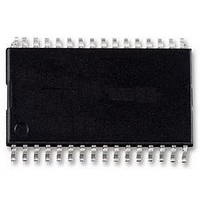
SRAM 4M, 512KX8, 2.4-5.5V, SOP32

BS62LV4006SIP55

Manufacturer Part Number
BS62LV4006SIP55
Description
SRAM 4M, 512KX8, 2.4-5.5V, SOP32
Manufacturer
BSI (BRILLIANCE SEMICONDUCTOR)
Datasheet

Specifications of BS62LV4006SIP55

Memory Size
4Mbit
Access Time
55ns
Supply Voltage Range
2.4V To 5.5V
Memory Case Style
SOP
No. Of Pins
32
Operating Temperature Range
-40°C To +85°C
Operating Temperature Max
85°C
Operating
RoHS Compliant

Available stocks

Company
Part Number
Manufacturer
Quantity
Price
Part Number:
BS62LV4006SIP55
Manufacturer:
BSI
Quantity:
2 051
Part Number:
BS62LV4006SIP55
Manufacturer:
BSI
Quantity:
20 000
GND
DQ0
DQ1
DQ2
n FEATURES
Ÿ Wide V
Ÿ Very low power consumption :
Ÿ High speed access time :
Ÿ Automatic power down when chip is deselected
Ÿ Easy expansion with CE and OE options
Ÿ Three state outputs and TTL compatible
Ÿ Fully static operation
Ÿ Data retention supply voltage as low as 1.5V
n POWER CONSUMPTION
n PIN CONFIGURATIONS
R0201-BS62LV4006
A18
A16
A14
A12
A7
A6
A5
A4
A3
A2
A1
A0
Brilliance Semiconductor, Inc.
V
V
-55
-70
BS62LV4006DC
BS62LV4006EC
BS62LV4006HC
BS62LV4006PC
BS62LV4006SC
BS62LV4006STC
BS62LV4006TC
BS62LV4006EI
BS62LV4006HI
BS62LV4006PI
BS62LV4006SI
BS62LV4006STI
BS62LV4006TI
CC
CC
1
2
3
4
5
6
7
8
9
10
11
12
13
14
15
16
PRODUCT
= 3.0V
= 5.0V
FAMILY
CC
BS62LV4006EC
BS62LV4006EI
BS62LV4006SC
BS62LV4006SI
BS62LV4006PC
BS62LV4006PI
operation voltage : 2.4V ~ 5.5V
VCC
A11
A13
A17
A15
A18
A16
A14
A12
WE
A9
A8
A7
A6
A5
A4
Operation current : 30mA (Max.) at 55ns
Standby current :
Operation current : 70mA (Max.) at 55ns
Standby current :
55ns (Max.) at V
70ns (Max.) at V
1
2
3
4
5
6
7
8
9
10
11
12
13
14
15
16
32
31
30
29
28
27
26
25
24
23
22
21
20
19
18
17
TEMPERATURE
-40
+0
OPERATING
BS62LV4006TC
BS62LV4006TI
BS62LV4006STC
BS62LV4006STI
VCC
A15
A17
WE
A13
A8
A9
A11
OE
A10
CE
DQ7
DQ6
DQ5
DQ4
DQ3
Commercial
O
Industrial
O
C to +70
C to +85
Pb-Free and Green package materials are compliant to RoHS
Very Low Power CMOS SRAM
512K X 8 bit
A
B
C
D
E
G
H
F
CC
CC
O
=3.0~5.5V
=2.7~5.5V
O
DQ4
DQ5
VSS
VCC
DQ6
DQ7
C
A0
A9
C
0.25uA (Typ.) at 25
10mA (Max.) at 1MHz
1.5uA (Typ.) at 25
1
2mA (Max.) at 1MHz
A10
A1
A2
OE
2
V
36-ball BGA top view
CC
10uA
20uA
32
31
30
29
28
27
26
25
24
23
22
21
20
19
18
17
=5.0V
WE
A18
A11
NC
NC
CE
STANDBY
3
(I
CCSB1
OE
A10
CE
DQ7
DQ6
DQ5
DQ4
DQ3
GND
DQ2
DQ1
DQ0
A0
A1
A2
A3
A17
A16
A12
A3
A4
A5
4
reserves the right to change products and specifications without notice.
, Max)
V
2.0uA
4.0uA
CC
A15
A13
A6
A7
5
=3.0V
O
O
C
C
DQ0
DQ1
VCC
DQ2
DQ3
VSS
A14
A8
6
10mA
1MHz
9mA
1
POWER DISSIPATION
n DESCRIPTION
The BS62LV4006 is a high performance, very low power CMOS
Static Random Access Memory organized as 524,288 by 8 bits and
operates form a wide range of 2.4V to 5.5V supply voltage.
Advanced CMOS technology and circuit techniques provide both
high speed and low power features with typical CMOS standby
current of 0.25uA at 3.0V/25
3.0V/85
Easy memory expansion is provided by an active LOW chip enable
(CE), and active LOW output enable (OE) and three-state output
drivers.
The BS62LV4006 has an automatic power down feature, reducing
the power consumption significantly when chip is deselected.
The BS62LV4006 is available in DICE form, JEDEC standard 32 pin
450mil Plastic SOP, 600mil Plastic DIP, 400 mil TSOP II,
8mmx13.4mm STSOP and 8mmx20mm TSOP package.
n BLOCK DIAGRAM
V
10MHz
43mA
45mA
CC
DQ0
DQ1
DQ2
DQ3
DQ4
DQ5
DQ6
DQ7
GND
A12
A14
A16
A18
A15
A17
A13
A11
=5V
WE
OE
V
A8
A9
CE
CC
O
C.
68mA
70mA
Address
f
Buffer
Max.
Input
Operating
Control
(I
CC
8
8
, Max)
1.5mA
10
1MHz
2mA
O
Output
Buffer
Buffer
Input
C and maximum access time of 55ns at
Data
Data
Decoder
Row
V
10MHz
18mA
20mA
CC
=3V
8
8
BS62LV4006
1024
29mA
30mA
A7
f
Max.
A6
Address Input Buffer
A5
Column Decoder
Memory Array
1024 x 4096
Write Driver
Revision
May.
Column I/O
Sense Amp
A4 A3 A2 A1 A0
DICE
TSOP II-32
BGA-36-0608
PDIP-32
SOP-32
STSOP-32
TSOP-32
TSOP II-32
BGA-36-0608
PDIP-32
SOP-32
STSOP-32
TSOP-32
PKG TYPE
4096
256
9
2006
A0
1.4

Related parts for BS62LV4006SIP55

BS62LV4006SIP55 Summary of contents

Page 1

Very Low Power CMOS SRAM 512K X 8 bit Pb-Free and Green package materials are compliant to RoHS n FEATURES Ÿ Wide V operation voltage : 2.4V ~ 5.5V CC Ÿ Very low power consumption : V = 3.0V Operation ...

Page 2

PIN DESCRIPTIONS Name A0-A18 Address Input CE Chip Enable Input WE Write Enable Input OE Output Enable Input DQ0-DQ7 Data Input/Output Ports V CC GND n TRUTH TABLE CE MODE Not selected H (Power Down) Output Disabled Read Write ...

Page 3

DC ELECTRICAL CHARACTERISTICS (T PARAMETER PARAMETER NAME V Power Supply CC V Input Low Voltage IL V Input High Voltage IH I Input Leakage Current IL I Output Leakage Current LO V Output Low Voltage OL V Output High ...

Page 4

AC TEST CONDITIONS (Test Load and Input/Output Reference) Input Pulse Levels Input Rise and Fall Times Input and Output Timing Reference Level CLZ OLZ CHZ OHZ WHZ Output Load Others ...

Page 5

SWITCHING WAVEFORMS (READ CYCLE) (1,2,4) READ CYCLE 1 ADDRESS D OUT (1,3,4) READ CYCLE OUT (1, 4) READ CYCLE 3 ADDRESS OUT NOTES high in read Cycle. 2. Device is ...

Page 6

AC ELECTRICAL CHARACTERISTICS (T WRITE CYCLE JEDEC PARANETER PARAMETER NAME NAME t t Write Cycle Time AVAX Chip Select to End of Write E1LWH Address Set up Time AVWL Address ...

Page 7

WRITE CYCLE 2 ADDRESS OUT D IN NOTES must be high during address transitions. 2. The internal write time of the memory is defined by the overlap of CE and WE low. All signals ...

Page 8

ORDERING INFORMATION BS62LV4006 Note: BSI (Brilliance Semiconductor Inc.) assumes no responsibility for the application or use of any product or circuit described herein. BSI does not authorize its products for use as critical components in any application in which ...

Page 9

PACKAGE DIMENSIONS (continued) STSOP - 32 TSOP - 32 R0201-BS62LV4006 9 BS62LV4006 Revision 1.4 May. 2006 ...

Page 10

PACKAGE DIMENSIONS (continued) PDIP - 32 D1 VIEW A 36 mini-BGA (6 x 8mm) R0201-BS62LV4006 NOTES : 1: CONTROLLING DIMENSIONS ARE IN MILLIMETERS. 2: PIN#1 DOT MARKING BY LASER OR PAD PRINT. 3: SYMBOL "N" IS THE NUMBER OF ...

Page 11

PACKAGE DIMENSIONS (continued SEATING PLANE -T- RAD R GAGE PLANE L RAD R1 L2 DETAIL "X" TSOP R0201-BS62LV4006 "X" NOTE: 1. CONTROLLING DIMENSION : MILLIMETERS. ...

Page 12

Revision History Revision No. History 1.2 To add Icc1 characteristic parameter To improve Iccsb1 spec. I-grade from 60uA to 20uA at 5.0V C-grade from 30uA to 10uA at 5.0V 1.3 To Add 400 mil TSOP II package type 1.4 ...

Related keywords