MCP1630RD-DDBK1 Microchip Technology, MCP1630RD-DDBK1 Datasheet - Page 7
MCP1630RD-DDBK1
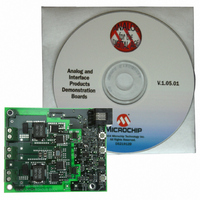
Manufacturer Part Number
MCP1630RD-DDBK1
Description
MCP1630 Dual Synchronous Buck Regulator Demo Board DEVTOOL - Analog
Manufacturer
Microchip Technology
Type
DC/DC Switching Converters, Regulators & Controllersr
Specifications of MCP1630RD-DDBK1
Main Purpose
DC/DC, Step Down
Outputs And Type
2, Non-Isolated
Voltage - Output
1.22 ~ 2.3V, 2.42 ~ 3.39V
Current - Output
20A, 20A
Voltage - Input
9 ~ 13.5V
Regulator Topology
Buck
Frequency - Switching
500kHz
Board Type
Fully Populated
Utilized Ic / Part
MCP1630
Input Voltage
12 V
Interface Type
Ethernet
Product
Power Management Modules
Lead Free Status / RoHS Status
Lead free / RoHS Compliant
Power - Output
-
Lead Free Status / Rohs Status
Lead free / RoHS Compliant
For Use With/related Products
MCP1630
Lead Free Status / RoHS Status
Lead free / RoHS Compliant, Contains lead / RoHS non-compliant


AC/DC CHARACTERISTICS (CONTINUED)
TEMPERATURE SPECIFICATIONS
© 2005 Microchip Technology Inc.
Electrical Specifications: Unless otherwise noted, V
V
Current Sense Input
Maximum Current Sense Signal
MCP1630
Delay From CS to V
MCP1630
Maximum Current Sense Signal
MCP1630V
Delay From CS to V
MCP1630V
Minimum Duty Cycle
Current Sense Input Bias Current
Internal Driver
R
R
V
V
Protection Features
Under Voltage Lockout
Under Voltage Lockout Hysteresis UVLO
Thermal Shutdown
Thermal Shutdown Hysteresis
Note 1:
Electrical Specifications: V
Temperature Ranges
Operating Junction Temperature Range
Storage Temperature Range
Maximum Junction Temperature
Thermal Package Resistances
Thermal Resistance, 8L-DFN
(2 mm x 3 mm)
Thermal Resistance, 8L-MSOP
IN
EXT
EXT
DSON
DSON
for typical values = 5.0V, T
Rise Time
Fall Time
2:
3:
P-channel
N-channel
Parameters
Capable of higher frequency operation depending on minimum and maximum duty cycles needed.
External oscillator input (OSC IN) rise and fall times between 10 ns and 10 µs used for characterization testing. Signal
levels between 0.8V and 2.0V with rise and fall times measured between 10% and 90% of maximum and minimum
values. Not production tested.
The reference input of the internal amplifier is capable of rail-to-rail operation.
Parameters
EXT
EXT
IN
A
= 3.0V to 5.5V, F
= -40°C to +125°C.
T
T
T
V
V
R
R
SHD_HYS
CS_VEXT
CS_VEXT
DC
UVLO
CS_MAX
CS_MAX
T
T
I
DSon_P
DSon_N
T
Sym
CS_B
RISE
FALL
SHD
MIN
HYS
Sym
T
T
T
JA
JA
OSC
A
A
J
0.85
2.55
Min
2.7
50
—
—
—
—
—
—
—
—
—
—
= 1 MHz with 10% Duty Cycle, C
IN
= 3.0V to 5.5V, F
Min
-40
-65
—
—
—
17.5
-0.1
Typ
150
0.9
2.7
5.9
6.2
12
10
75
18
—
—
7
50.8
Typ
208
—
—
—
MCP1630/MCP1630V
OSC
Max
0.95
2.85
150
3.0
25
35
—
30
30
18
18
—
—
0
+125
+150
+150
Max
= 1 MHz with 10% Duty Cycle, C
—
—
Units
Units
IN
°C/W
°C/W
mV
µA
°C
°C
ns
ns
ns
ns
%
V
V
V
°C
°C
°C
= 0.1 µF. T
Set by maximum error amplifier
clamp voltage, divided by 3.
V
Maximum CS input range limited by
comparator input common mode
range. V
V
V
V
C
Typical for V
C
Typical for V
V
UVLO
Steady state
Transient
Typical 4-layer board with two
interconnecting vias
Typical 4-layer board
IN
FB
CS
IN
IN
L
L
= 100 pF
= 100 pF
> 4.25V
= 5V
falling, V
= V
= GND
A
= -40°C to +125°C.
REF
CS_MAX
+ 0.1V,
IN
IN
EXT
Conditions
Conditions
= 3V
= 3V
IN
= V
low state when in
= 0.1 µF,
DS21896B-page 7
IN
-1.4V
Related parts for MCP1630RD-DDBK1
Image
Part Number
Description
Manufacturer
Datasheet
Request
R

Part Number:
Description:
REF DESIGN MCP1630 NIMH BATT CHG
Manufacturer:
Microchip Technology
Datasheet:

Part Number:
Description:
BOARD DEMO FOR MCP1630 LI-ION
Manufacturer:
Microchip Technology
Datasheet:

Part Number:
Description:
REF DESIGN MCP1630V BI-DIR 4CELL
Manufacturer:
Microchip Technology
Datasheet:

Part Number:
Description:
REFERENCE DESIGN FOR MCP1630
Manufacturer:
Microchip Technology
Datasheet:
Part Number:
Description:
Power Management IC Development Tools MCP1630 Sepic Automotive LED Drvr
Manufacturer:
Microchip Technology
Datasheet:

Part Number:
Description:
Manufacturer:
Microchip Technology Inc.
Datasheet:
Part Number:
Description:
Manufacturer:
Microchip Technology Inc.
Datasheet:
Part Number:
Description:
Manufacturer:
Microchip Technology Inc.
Datasheet:
Part Number:
Description:
Manufacturer:
Microchip Technology Inc.
Datasheet:
Part Number:
Description:
Manufacturer:
Microchip Technology Inc.
Datasheet:
Part Number:
Description:
Manufacturer:
Microchip Technology Inc.
Datasheet: