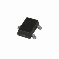
A1383LLHLT-T Allegro Microsystems Inc, A1383LLHLT-T Datasheet - Page 11

A1383LLHLT-T
Manufacturer Part Number
A1383LLHLT-T
Description
IC SENSOR HALL EFFECT SOT23-W
Manufacturer
Allegro Microsystems Inc
Series
A138xr
Type
Linear - Programmabler
Datasheet
1.A1381ELHLT-T.pdf
(19 pages)
Specifications of A1383LLHLT-T
Sensing Range
2.75mV/G ~ 4.25mV/G
Voltage - Supply
4.5 V ~ 5.5 V
Current - Supply
8mA
Current - Output (max)
10mA
Output Type
Analog, Ratiometric
Operating Temperature
-40°C ~ 150°C
Package / Case
SOT-23W
Peak Reflow Compatible (260 C)
Yes
Accuracy %
1.5%
Supply Voltage
5V
Output Current
2mA
Termination Type
SMD
Bandwidth
21kHz
Supply Voltage Max
5.5V
Sensitivity
2.75 To 4.25 MV/G
No. Of Pins
3
Hall Effect Type
Linear
Supply Voltage Min
4.5V
Operating Temperature Max
150°C
Rohs Compliant
Yes
Filter Terminals
SMD
Leaded Process Compatible
Yes
Operating Temperature Min
-40°C
Lead Free Status / RoHS Status
Lead free / RoHS Compliant
Features
-
Lead Free Status / RoHS Status
Lead free / RoHS Compliant, Lead free / RoHS Compliant
Other names
620-1198-2
A1381, A1382,
A1383, and A1384
Overview
Programming is accomplished by sending a series of input volt-
age pulses serially through the VOUT pin of the device. A unique
combination of different voltage level pulses controls the internal
programming logic of the device to select a desired program-
mable parameter and change its value. There are two program-
ming pulses, referred to as a high voltage pulse, V
of a V
pulse, V
The 138x features Try mode, Blow mode, and Lock mode:
•
•
•
The programming sequence is designed to help prevent the
device from being programmed accidentally; for example, as a
result of noise on the supply line.
Although any programmable variable power supply can be
used to generate the pulse waveforms, Allegro highly recom-
mends using the Allegro Sensor IC Evaluation Kit, available on
the Allegro Web site On-line Store. The manual for that kit is
available for download free of charge, and provides additional
information on programming these devices.
Programming Pulse Requirements, Protocol at T
Programming Voltage
Programming Current
In Try mode, the value of a single programmable parameter may
be set and measured. The parameter value is stored temporar-
ily, and resets after cycling the supply voltage. Note that other
parameters cannot be accessed simultaneously in this mode.
In Blow mode, the value of a single programmable parameter
may be permanently set by blowing solid-state fuses internal to
the device. Additional parameters may be blown sequentially.
In Lock mode, a device-level fuse is blown, blocking the fur-
ther programming of all parameters.
Characteristic
Pulse Rise Time
Pulse Fall Time
Pulse Width
P(LOW)
PM
, consisting of a V
–V
P(HIGH)
t
t
ACTIVE(HIGH)
ACTIVE(MID)
t
Symbol
–V
V
OFF(HIGH)
t
V
OFF(MID)
V
t
P(HIGH)
P(LOW)
BLOW
P(MID)
t
t
P(LOW)
I
Pr
Pf
P
P(LOW)
sequence and a mid voltage
Measured at the VOUT pin.
Minimum supply current required to ensure proper fuse blowing. In addition, a min-
imum capacitance, C
GND pins during programming to provide the current necessary for fuse blowing.
Duration at V
Duration at V
Duration of V
Duration of V
Duration at V
Rise time required for transitions from V
Fall time required for transitions from V
Programmable Linear Hall Effect Sensor ICs with Analog Output
–V
P(MID)
Available in a Miniature Thin Profile Surface Mount Package
–V
A
P(LOW)
P(LOW)
P(HIGH)
P(MID)
P(HIGH)
= 25°C
Programming Guidelines
P(LOW)
PH
level for V
, consisting
level following a V
level following a V
level for V
level for fuse blowing.
BLOW
sequence.
= 0.1 μF, must be connected between the VOUT and
PH
PH
pulses during key/code selection.
pulses during key/code selection.
Notes
P(HIGH)
P(MID)
Definition of Terms
Register. The section of the programming logic that controls the
choice of programmable modes and parameters.
Bit Field. The internal fuses unique to each register, represented
as a binary number. Incrementing the bit field of a particular
register causes its programmable parameter to change, based on
the internal programming logic.
Key. A series of V
a value expressed as the decimal equivalent of the binary value.
The LSB of a register is denoted as key 1, or bit 0.
Code. The number used to identify the combination of fuses
activated in a bit field, expressed as the decimal equivalent of the
binary value. The LSB of a bit field is denoted as code 1, or bit 0.
Addressing. Incrementing the bit field code of a selected register
by serially applying a pulse train through the VOUT pin of the
device. Each parameter can be measured during the addressing
process, but the internal fuses must be blown before the program-
ming code (and parameter value) becomes permanent.
Fuse Blowing. Applying a V
tion at the V
blowing a fuse internal to the device. Once a bit (fuse) has been
blown, it cannot be reset.
Blow Pulse. A V
V
Cycling the Supply. Powering-down, and then powering-up the
supply voltage. Cycling the supply is used to clear the program-
ming settings in Try mode.
P(HIGH)
P(LOW)
P(HIGH)
level.
level.
to either V
to either V
level to blow the addressed fuse.
P(HIGH)
P(MID)
P(MID)
PH
PM
voltage pulse of sufficient duration at the
level to permanently set an addressed bit by
to V
or V
voltage pulses used to select a register, with
P(LOW)
P(HIGH)
115 Northeast Cutoff, Box 15036
Allegro MicroSystems, Inc.
Worcester, Massachusetts 01615-0036 (508) 853-5000
www.allegromicro.com
PH
.
.
voltage pulse of sufficient dura-
Min. Typ. Max. Units
300
14
26
30
30
15
30
5
1
1
-
15
27
-
-
-
-
-
-
-
-
-
100
100
5.5
16
28
-
-
-
-
-
-
mA
μs
μs
μs
μs
μs
μs
μs
V
V
V
11


