A1321LUA-T Allegro Microsystems Inc, A1321LUA-T Datasheet - Page 2
A1321LUA-T
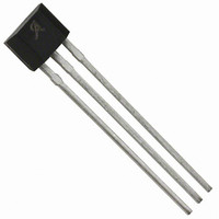
Manufacturer Part Number
A1321LUA-T
Description
IC SENSOR HALL EFFECT 3-SIP
Manufacturer
Allegro Microsystems Inc
Type
Linear - Ratiometricr
Datasheet
1.A1321ELHLT-T.pdf
(13 pages)
Specifications of A1321LUA-T
Sensing Range
4.75mV/G ~ 5.25mV/G
Voltage - Supply
4.5 V ~ 5.5 V
Current - Supply
8mA
Current - Output (max)
10mA
Output Type
Digital, Open Drain
Features
High Sensitivity
Operating Temperature
-40°C ~ 150°C
Package / Case
3-SIP
Peak Reflow Compatible (260 C)
Yes
Accuracy %
1.5%
Output Current
1mA
Termination Type
Through Hole
Bandwidth
30kHz
Supply Voltage Max
5.5V
Sensitivity
5 MV/G
No. Of Pins
3
Mounting Type
Through Hole
Hall Effect Type
Linear
Supply Voltage Min
4.5V
Rohs Compliant
Yes
Filter Terminals
Through Hole
Leaded Process Compatible
Yes
Lead Free Status / RoHS Status
Lead free / RoHS Compliant
Other names
620-1024


Features and Benefits
▪ Temperature-stable quiescent output voltage
▪ Precise recoverability after temperature cycling
▪ Output voltage proportional to magnetic flux density
▪ Ratiometric rail-to-rail output
▪ Improved sensitivity
▪ 4.5 to 5.5 V operation
▪ Immunity to mechanical stress
▪ Solid-state reliability
▪ Robust EMC protection
Packages: 3 pin SOT23W (suffix LH), and
3 pin SIP (suffix UA)
Not to scale
A1321-DS, Rev. 23
V+
0.1 F
VCC
Ratiometric Linear Hall Effect Sensor ICs
Functional Block Diagram
for High-Temperature Operation
Amp
Gain
A1321, A1322, and A1323
Description
The A132X family of linear Hall-effect sensor ICs are optimized,
sensitive, and temperature-stable. These ratiometric Hall-effect
sensor ICs provide a voltage output that is proportional to the
applied magnetic field. The A132X family has a quiescent
output voltage that is 50% of the supply voltage and output
sensitivity options of 2.5 mV/G, 3.125 mV/G, and 5m V/G.
The features of this family of devices are ideal for use in the
harsh environments found in automotive and industrial linear
and rotary position sensing systems.
Each device has a BiCMOS monolithic circuit which integrates
a Hall element, improved temperature-compensating circuitry
to reduce the intrinsic sensitivity drift of the Hall element,
a small-signal high-gain amplifier, and a rail-to-rail low-
impedance output stage.
A proprietary dynamic offset cancellation technique, with
an internal high-frequency clock, reduces the residual offset
voltage normally caused by device overmolding, temperature
dependencies, and thermal stress. The high frequency clock
allows for a greater sampling rate, which results in higher
accuracy and faster signal processing capability. This technique
produces devices that have an extremely stable quiescent output
voltage, are immune to mechanical stress, and have precise
Continued on the next page…
GND
Control
Offset
Out
Trim
VOUT
Related parts for A1321LUA-T
Image
Part Number
Description
Manufacturer
Datasheet
Request
R

Part Number:
Description:
IC SOCK 40 PIN HORIZ GOLD .600
Manufacturer:
Aries Electronics
Datasheet:

Part Number:
Description:
IC, HALL EFFECT SENSOR, Linear, SOIC-8
Manufacturer:
Allegro Microsystems Inc
Datasheet:
Part Number:
Description:
IC, HALL EFFECT SENSOR, Linear, SOIC-8
Manufacturer:
Allegro Microsystems Inc
Datasheet:
Part Number:
Description:
IC, HALL EFFECT SENSOR, Linear, SOIC-8
Manufacturer:
Allegro Microsystems Inc
Datasheet:

Part Number:
Description:
IC SWITCH INTERFACE 2CHAN 8-SOIC
Manufacturer:
Allegro Microsystems Inc
Datasheet:

Part Number:
Description:
IC SMOKE DETECTOR ION 16-DIP
Manufacturer:
Allegro Microsystems Inc
Datasheet:
Part Number:
Description:
IC SMOKE DETECTOR ION 16-DIP
Manufacturer:
Allegro Microsystems Inc
Datasheet:
Part Number:
Description:
IC SMOKE DETECTOR ION 16-DIP
Manufacturer:
Allegro Microsystems Inc
Datasheet:
Part Number:
Description:
IC SMOKE DETECTOR PHOTO 16-DIP
Manufacturer:
Allegro Microsystems Inc
Datasheet:
Part Number:
Description:
IC SMOKE DETECTOR ION 16-DIP
Manufacturer:
Allegro Microsystems Inc
Datasheet:
Part Number:
Description:
IC SMOKE DETECTOR PHOTO 16-DIP
Manufacturer:
Allegro Microsystems Inc
Datasheet:
Part Number:
Description:
IC SMOKE DETECTOR PHOTO 16-DIP
Manufacturer:
Allegro Microsystems Inc
Datasheet:
Part Number:
Description:
IC SMOKE DETECTOR ION 16-DIP
Manufacturer:
Allegro Microsystems Inc
Datasheet:
Part Number:
Description:
IC SMOKE DETECTOR PHOTO 16-SOIC
Manufacturer:
Allegro Microsystems Inc
Datasheet:

Part Number:
Description:
IC LED DRIVER HIGH BRIGHT 16-QFN
Manufacturer:
Allegro Microsystems Inc
Datasheet: