A3211EUA-T Allegro Microsystems Inc, A3211EUA-T Datasheet
A3211EUA-T
Specifications of A3211EUA-T


Related parts for A3211EUA-T


A3211EUA-T Summary of contents
Page 1
Features and Benefits ▪ Micropower operation ▪ Operation with north or south pole ▪ 2.5 to 3.5 V battery operation ▪ Chopper stabilized ▫ Superior temperature stability ▫ Extremely low switchpoint drift ▫ Insensitive to physical stress ▪ High ESD ...
Page 2
A3211 and A3212 Description (continued) This device includes on a single silicon chip a Hall-voltage gen- erator, small-signal amplifier, chopper sta tion, a latch, and a MOSFET output. Advanced CMOS processing is used to take advantage of ...
Page 3
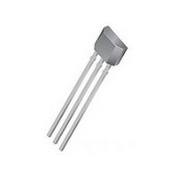
A3211 and A3212 Package Suffix ‘EH’ Pinning (Leadless Chip Carrier Package Suffix ‘LH’ Pinning (SOT23W Dwg. PH-016 Pinning is shown viewed from branded side. Micropower, Ultrasensitive Hall-Effect ...
Page 4
A3211 and A3212 ELECTRICAL CHARACTERISTICS Characteristic Supply Voltage Range Output Leakage Current Output On Voltage Awake Time Period Duty Cycle Chopping Frequency Supply Current * Typical data 25°C and V = 2.75 V, and is for ...
Page 5
A3211 and A3212 A3211 MAGNETIC CHARACTERISTICS Characteristic Symbol Over Temperature Range –40°C to 85° South pole to branded side; B > B OPS Operate Points B North pole to branded side; B > B OPN ...
Page 6
A3211 and A3212 TYPICAL OPERATING CHARACTERISTICS OPS B RPS 20 0 -20 B RPN -40 B OPN -60 -50 - AMBIENT TEMPERATURE IN ° ° ° ° C 7.0 6 =2.75 ...
Page 7
A3211 and A3212 Low Average Power. Internal timing circuitry activates the IC for 45 μs and deactivates it for the remainder of the period (45 ms). A short "awake" time allows for stabilization prior to the sam pling and data ...
Page 8
A3211 and A3212 Operation. The output of the A3212 switches low (turns on) when a magnetic field perpendicular to the Hall element exceeds the operate point B (or is less than B OPS output is capable of sinking up to ...
Page 9
A3211 and A3212 D 7X 0.08 C 0.25 ±0.05 0.5 BSC 0.55 ±0.10 For Reference Only, not for tooling use (reference DWG-2861; reference JEDEC MO-229WCED, Type 1) Dimensions in millimeters Exact case and lead configuration at supplier discretion within limits ...
Page 10
A3211 and A3212 E 2.00 ±0. 0.08 C +0.07 0.25 –0.05 0.40 ±0.05 For Reference Only, not for tooling use (reference DWG-2865; reference JEDEC MO-229UCCD) Dimensions in millimeters Exact case and lead configuration at supplier discretion within limits ...
Page 11
A3211 and A3212 +0.12 2.98 –0.08 3 +0.10 2.90 –0. 10° REF 0.95 BSC For Reference Only; not for tooling use (reference dwg. 802840) Dimensions in millimeters Dimensions exclusive of mold flash, gate burrs, and dambar protrusions Exact ...
Page 12
A3211 and A3212 4.09 45° +0.08 3.02 –0.05 2.16 MAX 0.51 REF 1 2 15.75 ±0.51 +0.05 0.43 –0.07 Copyright ©2002-2010, Allegro MicroSystems, Inc. Allegro MicroSystems, Inc. reserves the right to make, from time to time, such de par tures ...