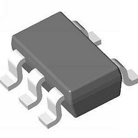
SIP21106DR-285-E3 Vishay, SIP21106DR-285-E3 Datasheet - Page 14

SIP21106DR-285-E3
Manufacturer Part Number
SIP21106DR-285-E3
Description
IC LDO REG 150MA 2.85V LN SC705L
Manufacturer
Vishay
Datasheet
1.SIP21106DR-33-E3.pdf
(15 pages)
Specifications of SIP21106DR-285-E3
Regulator Topology
Positive Fixed
Voltage - Output
2.85V
Voltage - Input
Up to 6V
Voltage - Dropout (typical)
0.16V @ 150mA
Number Of Regulators
1
Current - Output
150mA
Current - Limit (min)
170mA
Operating Temperature
-40°C ~ 85°C
Mounting Type
*
Package / Case
*
Number Of Outputs
1
Polarity
Positive
Input Voltage Max
6 V
Output Voltage
2.85 V
Output Type
Fixed
Dropout Voltage (max)
0.18 V at 150 mA
Output Current
150 mA
Line Regulation
0.2 % / V
Load Regulation
0.006 % / mA
Voltage Regulation Accuracy
1 %
Maximum Power Dissipation
0.187 W
Maximum Operating Temperature
+ 85 C
Mounting Style
SMD/SMT
Minimum Operating Temperature
- 40 C
Lead Free Status / RoHS Status
Lead free / RoHS Compliant
SiP21106, SiP21107, SiP21108
Vishay Siliconix
POK Status in SiP21107
The POK comparator monitors the output until the supply
comes up to specified percentage of V
NMOS output requires an external pull-up resistor to either
V
loads. POK pin is active high to indicate that output is within
percentage tolerance. POK goes low when output is outside
of this tolerance as when in dropout, over current and
thermal shutdown.
APPLICATION INFORMATION
Input/Output Capacitor Selection and Regulator Stability
It is recommended that a low ESR 1 µF capacitor be used on
the SiP21106, SiP21107, SiP21108 input. A larger input
capacitance with lower ESR would improve noise rejection
and line-transient response. A larger input bypass capacitor
may be required in applications involving long inductive
traces between the source and LDO. The circuit is stable with
only a small output capacitor equal to 6 nF/mA (≈ 1 µF at
150 mA) of load. Since the bandwidth of the error amplifier is
around 1 MHz - 3 MHz and the dominant pole is at the output
node, the capacitor should be capacitive in this range, i.e., for
150 mA load current, an ESR < 0.4 Ω is necessary. Parasitic
inductance of about 10 nH can be tolerated. Applying a larger
output capacitor would increase power supply rejection and
improve load-transient response. Some ceramic dielectrics
such as the Z5U and Y5V exhibit large capacitance and ESR
variation over temperature. If such capacitors are used, a
2.2 µF or larger value may be needed to ensure stability over
the industrial temperature range. If using higher quality
ceramic capacitors, such as those with X7R and Y7R
dielectrics, a 1 µF capacitor will be sufficient at all operating
temperatures.
Operating Region and Power Dissipation
An important consideration when designing power supplies
is the maximum allowable power dissipation of a part. The
maximum power dissipation in any application is dependant
on the maximum junction temperature, T
ambient temperature, T
thermal resistance for the package, which is the summation
of θ
thermal resistance through the PC board and copper traces.
Power dissipation may be expressed as:
Vishay Siliconix maintains worldwide manufacturing capability. Products may be manufactured at one of several qualified locations. Reliability data for Silicon
Technology and Package Reliability represent a composite of all qualified locations. For related documents such as package/tape drawings, part marking, and
reliability data, see
www.vishay.com
14
P
OUT
(max)
J-C
or V
, the thermal resistance of the package, and θ
=
IN
θ
T
. The internal NMOS can drive up to 0.5 mA
J
J-C
(max)
www.vishay.com/ppg?74442.
+
- T
θ
C-A
A
A
, and the junction-to-ambient
IN
J(max)
. This open drain
= 125 °C, the
C-A
, the
The GND pin of the SiP2110 acts as both the electrical
connection to GND as well as a path for channeling away
heat. Connect this pin to a GND plane to maximize heat
dissipation. Once maximum power dissipation is calculated
using the equation above, the maximum allowable output
current for any input/output potential can be calculated as
PCB Layout
The component placement around the LDO should be done
carefully to achieve good dynamic line and load response.
The input and noise capacitor should be kept close to the
LDO. The rise in junction temperature depends on how
efficiently the heat is carried away from junction-to-ambient.
The junction-to-lead thermal impedance is a characteristic of
the package and is fixed. The thermal impedance between
lead-to-ambient can be reduced by increasing the copper
area on PCB. Increase the input, output and ground trace
area to reduce the junction-to-ambient thermal impedance.
I
OUT(max)
=
V -
IN
P
(max)
V
OUT
S09-1047-Rev. G, 08-Jun-09
Document Number: 74442


