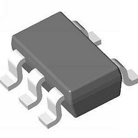
SIP21107DT-46-E3 Vishay, SIP21107DT-46-E3 Datasheet - Page 4

SIP21107DT-46-E3
Manufacturer Part Number
SIP21107DT-46-E3
Description
IC LDO REG 150MA 4.6V LN SC705L
Manufacturer
Vishay
Datasheet
1.SIP21106DR-33-E3.pdf
(15 pages)
Specifications of SIP21107DT-46-E3
Regulator Topology
Positive Fixed
Voltage - Output
4.6V
Voltage - Input
Up to 6V
Voltage - Dropout (typical)
0.16V @ 150mA
Number Of Regulators
1
Current - Output
150mA
Current - Limit (min)
170mA
Operating Temperature
-40°C ~ 85°C
Mounting Type
*
Package / Case
*
Number Of Outputs
1
Polarity
Positive
Input Voltage Max
6 V
Output Voltage
4.6 V
Output Type
Fixed
Dropout Voltage (max)
0.18 V at 150 mA
Output Current
150 mA
Line Regulation
0.2 % / V
Load Regulation
0.006 % / mA
Voltage Regulation Accuracy
1 %
Maximum Power Dissipation
0.305 W
Maximum Operating Temperature
+ 85 C
Mounting Style
SMD/SMT
Minimum Operating Temperature
- 40 C
Lead Free Status / RoHS Status
Lead free / RoHS Compliant
Available stocks
Company
Part Number
Manufacturer
Quantity
Price
Part Number:
SIP21107DT-46-E3
Manufacturer:
VISHAY/威世
Quantity:
20 000
SiP21106, SiP21107, SiP21108
Vishay Siliconix
Notes:
a. Room = 25 °C, Full = - 40 to 85 °C. Derate 7.6 mW/°C for TSC75 and 5.5 mW/°C for SOT23 above T
b. The algebraic convention whereby the most negative value is a minimum and the most positive a maximum.
c. Typical values are for DESIGN AID ONLY, not guaranteed nor subject to production testing.
d. Dropout voltage is defined as the input-to-output differential voltage at which the output voltage drops 2 % below its nominal
e. Ground current is specified for normal operation as well as “drop-out” operation.
f. Output noise is proportional to output voltage. Use formula e
g. POK threshold percentage is calculated by V
TIMING WAVEFORMS
www.vishay.com
4
turn on (low threshold) or off (high threshold). For V
SPECIFICATIONS
Parameter
Thermal Shutdown Junction Temperature
Thermal Hysteresis
Error Flag Section (SiP21107 Version only)
POK(OFF) Leakage
POK(ON) Voltage
POK Threshold
POK Hysteresis
POK Voltage Delay Time
value with constant load. For outputs = 2.2 V, dropout voltage is not applicable due to 2.2 V minimum input voltage requirement.
g
0 V
V
V
OUT
EN
IN
Symbol
T
/V
V
T
V
V
T
P_Delay
POKLH
I
J(S/D)
OUT
HYST
POKL
HYST
OFF
0.95 V
OUT
x 100 %. The POK is measured with a differential voltage across V
less than 2.2 V, POK is guaranteed functionality only.
t
NOM
ON
V
I
N
OUT
Test Conditions Unless Specified
IN
t
= 60 µV(rms)*V
V
r
V
V
falling, I
OUT
Figure 1.
OUT(nom)
OUT(nom)
= 1 mA, C
V
V
- 40 °C < T
OUT
OUT
1 µs
EN = 0 V, I
V
to POK delay, I
IN
R
rising, POK goes high
rising, POK goes high
= V
PU
OUT
≥ 2.2 V, I
< 2.2 V, I
to V
OUT(nom)
IN
= 1 mA, POK goes low
A
POK
= 1 µF, C
OUT
OUT
< 85 °C for full
= 0.5 mA
/2.8 V.
or V
OUT
OUT
OUT
+ 1.0 V
OUT
IN
= 1 mA
= 1 mA
= 1 mA
= 1 µF
V
V
IN
NOM
A
Temp.
= 70 °C.
Room
Room
Room
Full
Full
Full
a
S09-1047-Rev. G, 08-Jun-09
Min.
90
Document Number: 74442
b
IN
Typ.
160
1.5
20
93
91
40
and V
c
Max.
OUT
0.4
96
1
b
until POK
Unit
°C
µA
µs
%
V


