IRFB18N50KPBF Vishay, IRFB18N50KPBF Datasheet
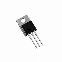
N CHANNEL MOSFET, 500V, 17A, TO-220

IRFB18N50KPBF

Manufacturer Part Number
IRFB18N50KPBF
Description
N CHANNEL MOSFET, 500V, 17A, TO-220
Manufacturer
Vishay
Type
Power MOSFETr

Specifications of IRFB18N50KPBF

Transistor Polarity
N Channel
Continuous Drain Current Id
17A
Drain Source Voltage Vds
500V
On Resistance Rds(on)
290mohm
Rds(on) Test Voltage Vgs
10V
Threshold Voltage Vgs Typ
5V
Fet Type
MOSFET N-Channel, Metal Oxide
Fet Feature
Standard
Rds On (max) @ Id, Vgs
290 mOhm @ 10A, 10V
Drain To Source Voltage (vdss)
500V
Current - Continuous Drain (id) @ 25° C
17A
Vgs(th) (max) @ Id
5V @ 250µA
Gate Charge (qg) @ Vgs
120nC @ 10V
Input Capacitance (ciss) @ Vds
2830pF @ 25V
Power - Max
220W
Mounting Type
Through Hole
Package / Case
TO-220-3 (Straight Leads)
Gate Charge Qg
120 nC
Minimum Operating Temperature
- 55 C
Configuration
Single
Resistance Drain-source Rds (on)
0.29 Ohm @ 10 V
Forward Transconductance Gfs (max / Min)
6.4 S
Drain-source Breakdown Voltage
500 V
Gate-source Breakdown Voltage
+/- 30 V
Continuous Drain Current
17 A
Power Dissipation
220000 mW
Maximum Operating Temperature
+ 150 C
Mounting Style
Through Hole
Number Of Elements
1
Polarity
N
Channel Mode
Enhancement
Drain-source On-res
0.29Ohm
Drain-source On-volt
500V
Gate-source Voltage (max)
±30V
Operating Temp Range
-55C to 150C
Operating Temperature Classification
Military
Mounting
Through Hole
Pin Count
3 +Tab
Package Type
TO-220AB
Lead Free Status / RoHS Status
Lead free / RoHS Compliant
Lead Free Status / RoHS Status
Lead free / RoHS Compliant, Lead free / RoHS Compliant
Other names
*IRFB18N50KPBF

Available stocks

Company
Part Number
Manufacturer
Quantity
Price
Part Number:
IRFB18N50KPBF
Manufacturer:
VISHAY/威世
Quantity:
20 000
Company:
Part Number:
IRFB18N50KPBF
Quantity:
1 500
Company:
Part Number:
IRFB18N50KPBF
Quantity:
70 000
Company:
Part Number:
IRFB18N50KPBF
Quantity:
25 780
Document Number: 91100
Applications
l
l
l
l
l
Benefits
l
l
l
l
Avalanche Characteristics
Thermal Resistance
Absolute Maximum Ratings
Symbol
R
R
R
I
I
I
P
V
dv/dt
T
T
Symbol
E
I
E
D
D
DM
AR
STG
D
GS
J
AS
AR
θJC
θCS
θJA
@ T
@ T
Switch Mode Power Supply (SMPS)
Uninterruptible Power Supply
High Speed Power Switching
Hard Switched and High Frequency
Lead-Free
Low Gate Charge Qg results in Simple Drive Requirement
Improved Gate, Avalanche and Dynamic dv/dt Ruggedness
Fully Characterized Capacitance and Avalanche Voltage
and Current
Low R
@T
Circuits
C
C
C
= 25°C
= 100°C
= 25°C
DS(on)
Junction-to-Case†
Case-to-Sink, Flat, Greased Surface
Junction-to-Ambient†
Continuous Drain Current, V
Pulsed Drain Current 
Power Dissipation
Linear Derating Factor
Gate-to-Source Voltage
Peak Diode Recovery dv/dt ƒ
Operating Junction and
Storage Temperature Range
Soldering Temperature, for 10 seconds
Mounting Torque, 6-32 or M3 screw
Single Pulse Avalanche Energy‚
Avalanche Current
Repetitive Avalanche Energy
(1.6mm from case )
Parameter
Parameter
Parameter
SMPS MOSFET
GS
GS
@ 10V
@ 10V
V
500V
IRFB18N50KPbF
DSS
Typ.
Typ.
0.50
–––
–––
–––
–––
–––
-55 to + 150
HEXFET Power MOSFET
Max.
220
± 30
300
1.8
7.8
17
11
68
10
R
DS(on)
0.26Ω
Max.
Max.
0.56
typ.
370
–––
58
17
22
TO-220AB
www.vishay.com
PD - 95472A
Units
W/°C
V/ns
°C
W
N
A
V
02/03/06
Units
Units
°C/W
17A
I
mJ
mJ
A
D
1

Related parts for IRFB18N50KPBF

IRFB18N50KPBF Summary of contents

Page 1

... AR Thermal Resistance Symbol Parameter R Junction-to-Case† θJC R Case-to-Sink, Flat, Greased Surface θCS R Junction-to-Ambient† θJA Document Number: 91100 SMPS MOSFET IRFB18N50KPbF HEXFET Power MOSFET V DSS 500V Max. @ 10V GS @ 10V GS - 150 Typ. ––– ––– ––– Typ. ...

Page 2

... 10V,See Fig. 10 „ 25V DS pF ƒ = 1.0MHz, See Fig 0V 1.0V, ƒ = 1.0MHz 0V 400V, ƒ = 1.0MHz 0V 400V … Conditions MOSFET symbol showing the integral reverse G p-n junction diode „ 25° 17A 25° 17A J F di/dt = 100A/µs „ µ DSS www.vishay.com ...

Page 3

... Fig 4. Normalized On-Resistance VGS 15V 12V 10V 8.0V 7.0V 6.0V 5.5V 5.0V 20µs PULSE WIDTH Tj = 150° Drain-to-Source Voltage (V) 17A V = 10V 100 120 140 160 ° Junction Temperature ( C) J Vs. Temperature www.vishay.com 100 3 ...

Page 4

... Single Pulse GS 0.1 10 1.1 1.4 Fig 8. Maximum Safe Operating Area 17A V = 400V 250V 100V 120 Q , Total Gate Charge (nC) G Gate-to-Source Voltage OPERATION IN THIS AREA LIMITED BY R DS(on) 10us 100us 1ms 10ms ° ° = 150 C 100 1000 V , Drain-to-Source Voltage (V) DS www.vishay.com 150 10000 4 ...

Page 5

... Fig 11. Maximum Effective Transient Thermal Impedance, Junction-to-Case Document Number: 91100 Fig 10a. Switching Time Test Circuit V DS 90% 125 150 ° 10 d(on) Fig 10b. Switching Time Waveforms Notes: 1. Duty factor Peak 0.001 0. Rectangular Pulse Duration (sec ≤ 1 ≤ 0 d(off thJC C 0.1 1 www.vishay.com 5 ...

Page 6

... Fig 13a. Gate Charge Test Circuit Document Number: 91100 I D TOP 7.6A 11A BOTTOM 17A 20V Fig 12c. Unclamped Inductive Test Circuit 125 150 ° Fig 12d. Unclamped Inductive Waveforms Fig 13b. Basic Gate Charge Waveform 15V DRIVER L D.U 0.01 Ω (BR)DSS Charge www.vishay.com A 6 ...

Page 7

... Inductor Curent * Fig 14. For N-Channel HEXFET Document Number: 91100 + • • ƒ • - „ - • • • • P.W. Period D = Period Body Diode Forward Current di/dt Waveform Diode Recovery dv/dt Body Diode Forward Drop Ripple ≤ 5% ® Power MOSFETs + + - * V =10V www.vishay.com 7 ...

Page 8

... IR WORLD HEADQUARTERS: 233 Kansas St., El Segundo, California 90245, USA Tel: (310) 252-7105 Document Number: 91100 Data and specifications subject to change without notice. This product has been designed and qualified for the industrial market. Qualification Standards can be found on IR’s Web site. TAC Fax: (310) 252-7903 02/06 www.vishay.com 8 ...

Page 9

... Except as provided in Vishay's terms and conditions of sale for such products, Vishay assumes no liability whatsoever, and disclaims any express or implied warranty, relating to sale and/or use of Vishay products including liability or warranties relating to fitness for a particular purpose, merchantability, or infringement of any patent, copyright, or other intellectual property right. ...

Related keywords