SI7112DN-T1-GE3 Vishay, SI7112DN-T1-GE3 Datasheet

N-CH 30-V (D-S) FAST SWITCHING MOSFE

SI7112DN-T1-GE3

Manufacturer Part Number
SI7112DN-T1-GE3
Description
N-CH 30-V (D-S) FAST SWITCHING MOSFE
Manufacturer
Vishay
Datasheet

Specifications of SI7112DN-T1-GE3

Fet Type
MOSFET N-Channel, Metal Oxide
Fet Feature
Logic Level Gate
Rds On (max) @ Id, Vgs
7.5 mOhm @ 17.8A, 10V
Drain To Source Voltage (vdss)
30V
Current - Continuous Drain (id) @ 25° C
11.3A
Vgs(th) (max) @ Id
1.5V @ 250µA
Gate Charge (qg) @ Vgs
27nC @ 4.5V
Input Capacitance (ciss) @ Vds
260pF @ 15V
Power - Max
1.5W
Mounting Type
Surface Mount
Package / Case
PowerPAK® 1212-8
Lead Free Status / RoHS Status
Lead free / RoHS Compliant
Other names
SI7112DN-T1-GE3TR

Available stocks

Company
Part Number
Manufacturer
Quantity
Price
Part Number:
SI7112DN-T1-GE3
Manufacturer:
VISHAY
Quantity:
10 646
Part Number:
SI7112DN-T1-GE3
Manufacturer:
VISHAY/威世
Quantity:
20 000
Company:
Part Number:
SI7112DN-T1-GE3
Quantity:
70 000
Notes:
a. Surface Mounted on 1" x 1" FR4 Board.
b. See Solder Profile (
copper (not plated) as a result of the singulation process in manufacturing. A solder fillet at the exposed copper tip cannot be guaranteed and is
not required to ensure adequate bottom side solder interconnection.
c. Rework Conditions: manual soldering with a soldering iron is not recommended for leadless components.
* Pb containing terminations are not RoHS compliant, exemptions may apply.
Document Number: 72864
S-60926-Rev. F, 29-May-06
ABSOLUTE MAXIMUM RATINGS T
Parameter
Drain-Source Voltage
Gate-Source Voltage
Continuous Drain Current (T
Pulsed Drain Current
Continuous Source Current (Diode Conduction)
Single Avalanche Current
Single Avalanche Energy
Maximum Power Dissipation
Operating Junction and Storage Temperature Range
Soldering Recommendations (Peak Temperature)
THERMAL RESISTANCE RATINGS
Parameter
Maximum Junction-to-Ambient
Maximum Junction-to-Case (Drain)
PRODUCT SUMMARY
V
DS
30
(V)
Ordering Information: Si7112DN-T1
8
3.30 mm
D
7
h
N-Channel 30-V (D-S) Fast Switching MOSFET
0.0082 at V
D
ttp://www.vishay.com/ppg?73257). The PowerPAK 1212-8 is a leadless package. The end of the lead terminal is exposed
0.0075 at V
6
PowerPAK 1212-8
D
r
DS(on)
J
a
5
Bottom View
= 150 °C)
a
D
Si7112DN-T1-E3 (Lead (Pb)-free)
GS
GS
(Ω)
= 4.5 V
= 10 V
1
S
a
2
S
3
a
S
b, c
3.30 mm
4
G
A
I
= 25 °C, unless otherwise noted
D
17.8
17.0
Steady State
Steady State
(A)
L = 0.1 mH
T
T
T
T
t ≤ 10 sec
A
A
A
A
= 25 °C
= 70 °C
= 25 °C
= 70 °C
FEATURES
APPLICATIONS
• TrenchFET
• New Low Thermal Resistance PowerPAK
• 100 % R
• Lead (Pb)-free Version is RoHS Compliant
• Synchronous Rectification
Symbol
Symbol
T
R
R
J
Package with Low 1.07 mm Profile
V
V
E
I
I
P
, T
I
DM
thJA
thJC
I
AS
DS
GS
AS
D
S
D
stg
g
Tested
®
Power MOSFET
Typical
10 sec
17.8
14.2
3.2
3.8
2.0
1.9
24
65
G
N-Channel MOSFET
- 55 to 150
± 12
260
30
60
20
20
Steady State
D
S
Maximum
11.3
9.1
1.3
1.5
0.8
2.4
33
81
Vishay Siliconix
Si7112DN
www.vishay.com
®
°C/W
Unit
Unit
RoHS*
mJ
COMPLIANT
°C
W
V
A
Available
1

Related parts for SI7112DN-T1-GE3

SI7112DN-T1-GE3 Summary of contents

Page 1

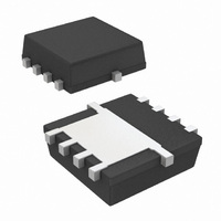
... V GS PowerPAK 1212 Bottom View Ordering Information: Si7112DN-T1 Si7112DN-T1-E3 (Lead (Pb)-free) ABSOLUTE MAXIMUM RATINGS T Parameter Drain-Source Voltage Gate-Source Voltage a Continuous Drain Current (T = 150 °C) J Pulsed Drain Current Continuous Source Current (Diode Conduction) Single Avalanche Current Single Avalanche Energy a Maximum Power Dissipation ...

Page 2

... Si7112DN Vishay Siliconix MOSFET SPECIFICATIONS T Parameter Static Gate Threshold Voltage Gate-Body Leakage Zero Gate Voltage Drain Current a On-State Drain Current a Drain-Source On-State Resistance a Forward Transconductance a Diode Forward Voltage b Dynamic Input Capacitance Output Capacitance Reverse Transfer Capacitance Total Gate Charge Gate-Source Charge ...

Page 3

... Source-Drain Diode Forward Voltage Document Number: 72864 S-60926-Rev. F, 29-May-06 3500 3000 2500 2000 1500 1000 0.040 0.035 0.030 0.025 0.020 0.015 °C 0.010 J 0.005 0.000 0.8 1.0 1.2 Si7112DN Vishay Siliconix C iss C oss C 500 rss Drain-to-Source Voltage (V) DS Capacitance 1 17 1.4 1.2 1.0 0.8 0 ...

Page 4

... Si7112DN Vishay Siliconix TYPICAL CHARACTERISTICS 25 °C unless noted 0 250 µA D 0.2 0.0 - 0.2 - 0.4 - 0 Temperature (°C) J Threshold Voltage 2 1 Duty Cycle = 0.5 0.2 0.1 0.1 0.05 0.02 Single Pulse 0. www.vishay.com 4 75 100 125 150 100 *Limited by r DS(on D(on) Limited ...

Page 5

... Package Reliability represent a composite of all qualified locations. For related documents such as package/tape drawings, part marking, and reliability data, see http://www.vishay.com/ppg?72864. Document Number: 72864 S-60926-Rev. F, 29-May- Square Wave Pulse Duration (sec) Normalized Thermal Transient Impedance, Junction-to-Case Si7112DN Vishay Siliconix - www.vishay.com 5 ...

Page 6

... Vishay disclaims any and all liability arising out of the use or application of any product described herein or of any information provided herein to the maximum extent permitted by law. The product specifications do not expand or otherwise modify Vishay’ ...

Related keywords