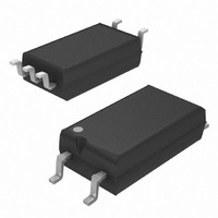
TCLT1109 Vishay, TCLT1109 Datasheet - Page 2
TCLT1109
Manufacturer Part Number
TCLT1109
Description
OPTOCOUPLER, TRANSISTOR, 5000VRMS
Manufacturer
Vishay
Specifications of TCLT1109
No. Of Channels
1
Optocoupler Output Type
Phototransistor
Input Current
50mA
Output Voltage
70V
Opto Case Style
SOP
No. Of Pins
5
Propagation Delay
3µs
Isolation Voltage
5kV
Number Of Channels
1
Input Type
DC
Voltage - Isolation
5000Vrms
Current Transfer Ratio (min)
200% @ 5mA
Current Transfer Ratio (max)
400% @ 5mA
Voltage - Output
70V
Current - Output / Channel
50mA
Current - Dc Forward (if)
60mA
Vce Saturation (max)
300mV
Output Type
Transistor with Base
Mounting Type
Surface Mount
Package / Case
6-SOP (5 Leads)
Maximum Input Diode Current
60 mA
Maximum Reverse Diode Voltage
6 V
Output Device
Transistor With Base
Configuration
1
Maximum Collector Emitter Voltage
70 V
Maximum Collector Emitter Saturation Voltage
300 mV
Current Transfer Ratio
400 %
Maximum Forward Diode Voltage
1.6 V
Maximum Collector Current
50 mA
Maximum Power Dissipation
250 mW
Maximum Operating Temperature
+ 100 C
Minimum Operating Temperature
- 40 C
Approval Bodies
BSI, DIN & FIMKO
Rohs Compliant
Yes
Lead Free Status / RoHS Status
Lead free / RoHS Compliant
Lead Free Status / RoHS Status
Lead free / RoHS Compliant, Lead free / RoHS Compliant
Available stocks
Company
Part Number
Manufacturer
Quantity
Price

Part Number:
TCLT1109
Manufacturer:
VISHAY/威世
Quantity:
20 000


TCLT11.. Series
Vishay Semiconductors
Absolute Maximum Ratings
T
Stresses in excess of the absolute Maximum Ratings can cause permanent damage to the device. Functional operation of the device is
not implied at these or any other conditions in excess of those given in the operational sections of this document. Exposure to absolute
Maximum Rating for extended periods of the time can adversely affect reliability.
Input
Output
Coupler
Electrical Characteristics
T
Minimum and maximum values are testing requirements. Typical values are characteristics of the device and are the result of engineering
evaluation. Typical values are for information only and are not part of the testing requirements.
Input
Output
www.vishay.com
2
Reverse voltage
Forward current
Forward surge current
Power dissipation
Junction temperature
Collector emitter voltage
Emitter collector voltage
Collector current
Collector peak current
Power dissipation
Junction temperature
Isolation test voltage (RMS)
Total power dissipation
Operating ambient temperature
range
Storage temperature range
Soldering temperature
Forward voltage
Junction capacitance
Collector emitter voltage
Emitter collector voltage
Collector-emitter cut-off current
amb
amb
= 25 °C, unless otherwise specified
= 25 °C, unless otherwise specified
Parameter
Parameter
Parameter
Parameter
Parameter
t
t
I
V
I
I
V
p
p
F
C
E
R
CE
/T = 0.5, t
≤ 10 µs
= ± 50 mA
= 100 µA
= 1 mA
= 0 V, f = 1 MHz
= 20 V, I
Test condition
Test condition
Test condition
Test condition
Test condition
p
≤ 10 ms
f
= 0, E = 0
Symbol
Symbol
V
V
I
CEO
V
CEO
ECO
C
F
j
Symbol
Symbol
Symbol
V
V
P
P
T
I
V
T
I
P
T
FSM
V
CEO
ECO
CM
amb
T
I
T
I
diss
diss
ISO
stg
sld
F
C
tot
R
j
j
Min
Min
70
7
- 40 to + 100
- 40 to + 100
Value
Value
Value
5000
1.25
Typ.
Typ.
100
125
100
150
125
250
240
1.5
60
70
50
50
10
6
7
Document Number 83514
Max
Max
100
1.6
Rev. 1.6, 20-Apr-04
VISHAY
V
Unit
mW
Unit
mW
Unit
mW
mA
mA
mA
RMS
°C
°C
°C
°C
°C
V
A
V
V
Unit
Unit
pF
nA
V
V
V
Related parts for TCLT1109
Image
Part Number
Description
Manufacturer
Datasheet
Request
R

Part Number:
Description:
Optocoupler/ Phototransistor Output/ SOP-6L5/ Half Pitch/ Long Mini-Flat Package
Manufacturer:
Vishay Siliconix
Datasheet:

Part Number:
Description:
357-036-542-201 CARDEDGE 36POS DL .156 BLK LOPRO
Manufacturer:
Vishay
Datasheet:
Part Number:
Description:
357-036-542-201 CARDEDGE 36POS DL .156 BLK LOPRO
Manufacturer:
Vishay
Datasheet:
Part Number:
Description:
357-036-542-201 CARDEDGE 36POS DL .156 BLK LOPRO
Manufacturer:
Vishay
Datasheet:
Part Number:
Description:
357-036-542-201 CARDEDGE 36POS DL .156 BLK LOPRO
Manufacturer:
Vishay
Datasheet:
Part Number:
Description:
357-036-542-201 CARDEDGE 36POS DL .156 BLK LOPRO
Manufacturer:
Vishay
Datasheet:
Part Number:
Description:
357-036-542-201 CARDEDGE 36POS DL .156 BLK LOPRO
Manufacturer:
Vishay
Datasheet:
Part Number:
Description:
357-036-542-201 CARDEDGE 36POS DL .156 BLK LOPRO
Manufacturer:
Vishay
Datasheet:
Part Number:
Description:
357-036-542-201 CARDEDGE 36POS DL .156 BLK LOPRO
Manufacturer:
Vishay
Datasheet:
Part Number:
Description:
357-036-542-201 CARDEDGE 36POS DL .156 BLK LOPRO
Manufacturer:
Vishay
Datasheet:
Part Number:
Description:
357-036-542-201 CARDEDGE 36POS DL .156 BLK LOPRO
Manufacturer:
Vishay
Datasheet:
Part Number:
Description:
357-036-542-201 CARDEDGE 36POS DL .156 BLK LOPRO
Manufacturer:
Vishay
Datasheet:
Part Number:
Description:
357-036-542-201 CARDEDGE 36POS DL .156 BLK LOPRO
Manufacturer:
Vishay
Datasheet:
Part Number:
Description:
357-036-542-201 CARDEDGE 36POS DL .156 BLK LOPRO
Manufacturer:
Vishay
Datasheet:
Part Number:
Description:
357-036-542-201 CARDEDGE 36POS DL .156 BLK LOPRO
Manufacturer:
Vishay
Datasheet: