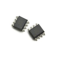
ACPL-0820-000E Avago Technologies US Inc., ACPL-0820-000E Datasheet - Page 9

ACPL-0820-000E
Manufacturer Part Number
ACPL-0820-000E
Description
Dual Line Driver,LF
Manufacturer
Avago Technologies US Inc.
Type
Driverr
Datasheet
1.ACPL-0820-500E.pdf
(10 pages)
Specifications of ACPL-0820-000E
Number Of Drivers/receivers
2/0
Voltage - Supply
4.75 V ~ 5.25 V
Mounting Type
Surface Mount
Package / Case
SO-8
Supply Voltage (max)
5.25 V
Supply Voltage (min)
4.75 V
Maximum Operating Temperature
+ 85 C
Mounting Style
SMD/SMT
Minimum Operating Temperature
- 40 C
Supply Current
40 mA
Lead Free Status / RoHS Status
Lead free / RoHS Compliant
Protocol
-
Lead Free Status / Rohs Status
Details
V
V
V
V
inp
inn
inp
inn
Test Circuit Diagrams
Unless otherwise noted, all test circuits are at T
132 kHz.
Figure 13. Load detection test circuit.
Figure 15. Tx enable/disable time test circuit.
Application Information
ACPL-0820 is designed to work with various transceivers
and can be used with a variety of modulation methods
including ASK, FSK and BPSK. Figure 17 shows a typical
Figure 17. Schematic of Isolated ACPL-0820 application for FSK modulation scheme.
9
=1.25V
=3.25V
= 1.25V
= 1.25V
Scope
*V
180
PLM Transceiver
inp
V
f
pulse
o
pulse
dc
dc
& V
out of phase
pp
pp
= 2.5kHz
STATUS
= 5V
inn
TX-EN
are
100nF
100nF
TXp
TXn
Pulse Gen.
10k
10k
5V
Ω
Ω
+
-
2k7 Ω�
Filter
10k
10k
5V
Ω
Ω
1
2
3
4
Status
In1
In2
Tx -en
1
2
3
4
100nF
100nF
C1
C2
Status
In1
In2
Tx -en
ACPL -0820
ACPL -0820
R1
R2
R 8
Out1
Out2
2k7
Gnd
Vdd
Out1
Out2
Gnd
Vdd
5V
10k Ω
10k Ω
20k
8
7
6
5
20k
20k
8
7
6
5
20k
Ω
Ω
100nF
Ω
Ω
1
2
3
4
100nF
Status
In1
In2
Tx -en
ACPL-0820
1
µ
1
µ
F
5V
F
5V
1
A
µ
F x2
Out1
Out2
Gnd
= 25°C, V
Vdd
I
I
out1
out2
V
50kΩ
8
7
6
5
R
R
50kΩ
out
R3
R4
R
R
L1
L2
L1
L2
100nF
C7
DD
C8
= 5 V, sinusoidal waveform input, and signal frequency f =
1µ F
f = 10k ~ 10MHz
Figure 14. Gain bandwidth product & Over Temp test circuit.
Figure 16. Tx-out harmonic distortion test circuit.
transformer isolated line driving application in a powerline
modem using Frequency Shift Keying (FSK) modulation
scheme.
V
V
Scope
*V
180
inp
inn
*V
out of phase
=1.75V
=1.75V
inp
inp
5V
V
V
o
inp
inn
& V
& V
out of phase
inn
pp
pp
inn
are 180
R5
1
R6
1
are
100nF
100nF
100nF
100nF
o
5V
2k7
5V
C3
1µ F
C4
1µ F
10k
10k
Ω
10kΩ
5V
10k Ω
Ω
Ω
L1
L2
1
2
3
4
1
2
3
4
Status
In1
In2
Tx -en
Status
In1
In2
Tx -en
ACPL -0820
ACPL -0820
TVS
TVS
5V
5V
Out1
Out2
D1
D2
Out1
Out2
Gnd
Vdd
Transformer
Gnd
Vdd
Signal
1:1
20k Ω
8
7
6
5
20k Ω
20k
8
7
6
5
20k
TVS
100nF
7V
Ω
Ω
D3
100nF
Type X2
Type X2
470nF
470nF
1µ F
C5
C6
1
µ
5V
F
5V
4µ 7F
4µ 7F
1
µ
F x2
220kΩ
V
V
R7
out1
out2
50Ω
Spectrum
Analyzer
V
L
N
out
R
R
L2
L1


