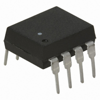
HCNW4504 Avago Technologies US Inc., HCNW4504 Datasheet

HCNW4504
Specifications of HCNW4504
Available stocks
Related parts for HCNW4504
HCNW4504 Summary of contents
Page 1
... RoHS 6 fully compliant options available; -xxxE denotes a lead-free product Description The HCPL-4504 and HCPL-0454 contain a GaAsP LED while the HCPL-J454 and HCNW4504 contain an AlGaAs LED. The LED is optically coupled to an integrated high gain photo detector. The HCPL-4504 series has short propagation delays and high CTR. The HCPL-4504 series also has a guaranteed propagation delay diff ...
Page 2
... Ordering Information HCPL-0454, HCPL-4504 and HCPL-J454 are UL Recognized with 3750 Vrms for 1 minute per UL1577. HCNW4504 is UL Recognized with 5000 Vrms for 1 minute per UL1577. HCPL-0454, HCPL-4504, HCPL-J454 and HCNW4504 are approved under CSA Component Acceptance Notice #5, File CA 88324. Option Part ...
Page 3
Package Outline Drawings HCPL-4504 Outline Drawing 9.65 ± 0.25 (0.380 ± 0.010 TYPE NUMBER A XXXXZ R U YYWW 1.19 (0.047) MAX. 3.56 ± 0.13 (0.140 ± 0.005) 1.080 ± 0.320 (0.043 ± 0.013) ...
Page 4
Package Outline Drawings HCPL-J454 Outline Drawing 9.80 ± 0.25 (0.386 ± 0.010 TYPE NUMBER A XXXX R U YYWW 1.19 (0.047) MAX. 3.56 ± 0.13 (0.140 ± 0.005) 1.080 ± 0.320 (0.043 ± 0.013) ...
Page 5
HCPL-J454-400E/600E Widelead Gullwing Surface Mount Outline Drawing 9.80 ±0.25 0.386 ±0.010 TYPE NUMBER A XXXX DATE CODE YYWW R [0.65] 0.025 MAX [1.19] 0.047 MAX. [1.080] 0.320 0.043 0.013 0.100 DIMENSIONS IN [MILLIMETERS] INCHES OPTION NUMBERS 400 AND 600 NOT ...
Page 6
... A HCNWXXXX YYWW 2.54 (0.100) TYP. 1.78 ± 0.15 (0.070 ± 0.006) HCNW4504 Gull Wing Surface Mount Option 300 Outline Drawing 11.15 ± 0.15 (0.442 ± 0.006 1.78 ± 0.15 (0.070 ± 0.006) 2.54 (0.100) BSC DIMENSIONS IN MILLIMETERS (INCHES). ...
Page 7
Solder Refl ow Temperature Profi le 300 PREHEATING RATE 3 ° °C/–0.5 °C/SEC. REFLOW HEATING RATE 2.5 °C ± 0.5 °C/SEC. 200 160 °C 150 °C 140 °C 3 ° °C/–0.5 °C 100 ROOM TEMPERATURE 0 ...
Page 8
... Creepage and clear- ance distances will also change depending on factors such as pollution degree and insulation level. HCPL-0454 HCNW4504 3750 Vrms / 5000 Vrms / 1 minute 1 minute 3750 Vrms / ...
Page 9
... V 840 945 PR V 4000 6000 IOTM T 150 175 S I 150 230 S,INPUT P 600 600 S,OUTPUT ≥10 ≥10 S HCPL-J454 HCNW4504 Unit I-IV I-IV I-IV I-IV I-III I-IV I-III I-IV I-III 55/100/21 55/85/ 891 1414 V peak 1670 2652 V peak 1336 2121 V peak 6000 ...
Page 10
... I F(AVG) I HCPL-4504 F(PEAK) HCPL-0454 HCPL-J454 HCNW4504 I HCPL-4504 F(TRANS) HCPL-0454 HCPL-J454 HCNW4504 V HCPL-4504 R HCPL-0454 HCPL-J454 HCNW4504 P HCPL-4504 IN HCPL-0454 HCPL-J454 HCNW4504 I O(AVG) I O(PEAK HCPL-4504 LS HCPL-J454 HCNW4504 T HCPL-0454, See Package Outline Drawings RP Option 300 , Option 500, Option 400E & Option 600E. Max. ...
Page 11
... HCPL-J454 Logic High I CCH Supply Current Input Forward V HCPL-4504 F Voltage HCPL-0454 HCPL-J454 HCNW4504 Input Reverse BV HCPL-4504 R Breakdown HCPL-0454 Voltage HCPL-J454 HCNW4504 Temperature ∆V HCPL-4504 F Coeffi cient HCPL-0454 ∆ Forward HCPL-J454 Voltage HCNW4504 Input C HCPL-4504 IN Capacitance HCPL-0454 HCPL-J454 HCNW4504 *All typicals 25° ...
Page 12
AC Switching Specifi cations Over recommended temperature (T = 0°C to 70°C) unless otherwise specifi ed. A Parameter Symbol Device Propagation Delay t PHL Time to Logic Low at Output t PHL HCPL- J454 Others 0.1 Propagation Delay t PLH ...
Page 13
... HCPL-4504 I-O (Input-Output) HCPL-0454 HCPL-J454 HCNW4504 All typicals 25°C.. A †The Input-Output Momentary Withstand Voltage is a dielectric voltage rating that should not be interpreted as an input-output continuous voltage rating. For the continuous voltage rating refer to the IEC/EN/DIN EN 60747-5-2 Insulation Related Characteristics Table (if applicable), your equipment level safety specifi ...
Page 14
... INPUT CURRENT – HCPL-J454/HCNW4504 1000 T = 25°C A 100 – 1.0 0.1 0.01 0.001 1.2 1.3 1.4 1.5 1.6 1.7 V – FORWARD VOLTAGE – VOLTS F HCNW4504 T = 25° 5 – OUTPUT VOLTAGE – HCNW4504 NORMALIZED 25°C A 1.2 0.8 0 – INPUT CURRENT – ...
Page 15
... NORMALIZED 25° 0.95 0.9 0.85 -60 -40 - 100 T – TEMPERATURE – ° PULSE F 1 GEN Ω MONITOR – PULSE GEN. HCNW4504 1.05 NORMALIZED 0 5 25°C A 0.95 0.9 0.85 -60 -40 - 100 120 T – TEMPERATURE – ° 0.1µ 0.1µ ...
Page 16
... 1.5 V THHL THLH 1.0 10% DUTY CYCLE t PLH 0.8 0 PHL 0 0.2 0 – LOAD RESISTANCE – kΩ L Figure 9. Propagation delay time vs. load resis- tance. HCPL-J454/HCNW4504 1 15 kΩ 1 100 1.5 V THHL t PLH V = 2.0 V THLH 0.8 50% DUTY CYCLE 0.7 0.6 0.5 t PHL 0.4 0.3 ...
Page 17
... LED HCPL-4504/0454/J454 8 HCNW4504 2 7 LED Figure 16. Typical power inverter. 17 HCPL-0454 OPTION 060/HCNW4504 1000 P (mW) for HCNW4504 S 900 I (mA) for HCNW4504 S P (mW) for HCPL-0454 S 800 OPTION 060 I (mA) for HCPL-0454 700 S OPTION 060 600 500 400 300 200 (150) 100 100 ...
Page 18
... Figure 17. LED delay and dead time diagram. Power Inverter Dead Time and Propagation Delay Specifi ca- tions The HCPL-4504/0454/J454 and HCNW4504 include a specifi ca tion intended to help designers minimize “dead time” in their power inverter designs. The new “propaga- tion delay diff erence” specifi cation (t deter min ing not only how much optocoupler switch- ing delay is needed to prevent “ ...
Page 19
... PLHmax PHLmin imum data sheet value for the propagation delay diff er- ence specifi cation The HCPL-4504/0454/J454 PLH PHL and HCNW4504 specify a maxi mum (t over an operating temperature range of 0-70°C. Although ( tells the designer how much delay PLH PHL max is needed to prevent shoot-through current insuffi ...


