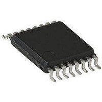
SI9118DB Vishay, SI9118DB Datasheet - Page 8

SI9118DB
Manufacturer Part Number
SI9118DB
Description
Pulse Width Modulation (PWM) Controller IC
Manufacturer
Vishay
Datasheet
1.SI9118DY-T1.pdf
(10 pages)
Specifications of SI9118DB
Silicon Manufacturer
Vishay
Application Sub Type
Pulse Width Modulation (PWM) Controller
Kit Application Type
Power Management
Silicon Core Number
SI9118
Kit Contents
Board
Lead Free Status / RoHS Status
Contains lead / RoHS non-compliant
Si9118/Si9119
Vishay Siliconix
DETAILED OPERATIONAL DESCRIPTION
Start-Up
Si9118/Si9119 are designed with internal depletion
mode MOSFET capable of powering directly from the
high input bus voltage. This feature eliminates the typ-
ical external start-up circuit saving valuable space and
cost. But, most of all, this feature improves the con-
verter efficiency during full load and has an even
greater impact on light load. With an input bus voltage
applied to the +V
9.3 V. The UVLO circuit prevents the controller output
driver section from turning on, until V
exceeds 8.7 V. In order to maximize converter effi-
ciency, the designer should provide an external boot-
strap winding to override the internal V
external VCC voltage is greater than 9.3 V, the internal
depletion mode MOSFET regulator is disabled and
power is derived from the external V
V
well as providing supply voltage to the gate drive cir-
cuit.
Soft-Start/Enable
The soft-start time is externally programmable with
capacitor connected to the SS/EN pin. A constant cur-
rent source provides the current to the SS/EN pin to
generate a linear start-up time versus the capacitance
value. The SS/EN pin clamps the error amplifier output
voltage, limiting the rate of increase in duty cycle. By
controlling the rate of rise in duty cycle gradually, the
output voltage rises gradually preventing the output
voltage from overshooting. The SS/EN pin can also be
used to enable or disable the output driver section with
an external logic signal.
Synchronization
The synchronization to external clock is easily accom-
plished by connecting the external clock into the SYNC
pin (Si9119 only). The logic high to low transition syn-
chronizes the clock. The external clock frequency must
be at least 5 % faster than the internal clock frequency.
Reference Voltage
The reference voltage for the Si9118/Si9119 are set at
4.0 V. The reference voltage is not connected to the
non-inverting inputs of the error amplifier, therefore,
the minimum output voltage is not limited to reference
voltage. The V
capacitor.
Error Amplifier
The error amplifier gain-bandwidth product is critical
parameter which determines the transient response of
converter. The transient response is function of both
www.vishay.com
8
CC
supply provides power to the internal circuity as
REF
IN
pin, the V
pin requires a 0.1 µF decoupling
CC
voltage is regulated to
CC
CC
supply. The
CC
regulator. If
voltage
small and large signal responses. The small signal
response is determined by the feedback compensation
network while the large signal response is determined
by the inductor di/dt slew rate. Besides the inductance
value, the error amplifier gain-bandwidth determine the
converter response time. In order to minimize the
response time, Si9118/Si9119 is designed with a
2.7 MHz error amplifier gain-bandwidth product to pro-
vide the widest converter bandwidth possible.
PWM Mode
The converter operates in PWM mode if the PWM/
PSM pin is connected to V
load current and line voltage vary, the Si9118/Si9119
maintain constant switching frequency until they reach
minimum duty cycle. Once the output voltage regula-
tion is exceeded with minimum duty cycle, the switch-
ing frequency will continue to decrease until regulation
is achieved. The switching frequency is controlled by
the external R
oscillator frequency curve. In PWM mode, output ripple
noise is constant reducing EMI concerns as well as
simplifying the filter to minimize the system noise.
Pulse Skipping Mode
If the PWM/PSM pin is connected to -V
low), the converter can operate in either PWM or PSM
mode depending on the load current. The converter
automatically transitions from PWM to PSM or vise
versa to maintain output voltage regulation. In PSM
mode, the MOSFET switch is turned on until the peak
current sensed voltage reaches 100 mV and the output
voltage meets or exceeds its regulation voltage. The
converter is operating in pulse skipping mode because
each pulse delivers excess energy into the output
capacitor forcing the output voltage to exceed its regu-
lation voltage. By forcing the output voltage to exceed
the regulation voltage, succeeding pulses are skipped
until the output voltage drops below the regulation
point. Therefore, switching frequency will continue to
reduce during PSM control as the demand for output
current decreases. The pulse skipping mode cuts
down the switching losses, the dominant power con-
sumed during low output current, thereby maintaining
high efficiency throughout the entire load range. With
PWM/PSM pin in logic low state, the converter transi-
tions back into PWM mode, if the peak current sensed
voltage of 100 mV does not generate the required out-
put voltage. In the region between pulse skipping
mode and PWM mode, the controller may transition
between the two modes, delivering spurts of pulses.
This may cause the current waveform to look irregular,
but this will not overly affect the ripple voltage. Even in
this transitional mode, efficiency remains high.
osc
and C
osc
REF
as shown by the typical
pin or logic high. As the
S-60550–Rev. D, 3-Apr-06
Document Number: 70815
IN
pin (logic


