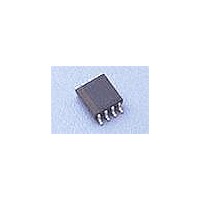
HV833MG Supertex, HV833MG Datasheet

HV833MG
Specifications of HV833MG
Available stocks
Related parts for HV833MG
HV833MG Summary of contents
Page 1
... Supertex inc. High Voltage EL Lamp Driver General Description The Supertex HV833 is a high voltage driver designed for driving EL lamps 35nF (10-12in 1.8 to 6.5V. The device uses a single inductor and a minimum number of passive components. The nominal regulated output voltage that is applied to the EL lamp is ±90V. The chip can be enabled/disabled by connecting a resistor between the RSW-Osc pin and the VDD/GND pins ...
Page 2
... EL DIFF F Switching transistor frequency SW D Switching transistor duty cycle Supertex inc. Pin Configuration 0.65mm pitch HV833MG-G Product Marking Value -0.5V to 7.5V -0.5V to 125V -40°C to +85°C -65°C to +150°C Package may or may not include the following marks 300mW Min Typ 1 ...
Page 3
... Enable/Disable Function Table Sym Parameter EN-L Logic input low voltage EN-H Logic input high voltage Functional Block Diagram VDD RSW-Osc GND REL-Osc Supertex inc. Min Typ 0.5 DD Switch Osc Disable V REF 1235 Bordeaux Drive, Sunnyvale, CA 94089 3 Max Units Conditions - 0 1.8 to 6.5V ...
Page 4
... Fig. 1: Typical Application/Test Circuit OFF = 4.7µ Typical Performance Device Lamp Size HV833MG 10in 2 Typical Performance Curves for Fig 100 200 V vs 1.0 2.0 3.0 4.0 V (V) IN Brightness vs 1.0 2.0 3.0 4.0 V (V) IN Supertex inc 3.3V Enable Signal VDD VA 8 1.0M ...
Page 5
... Fig. 2: Typical Application OFF = 4.7µ Typical Performance Device Lamp Size HV833MG 6.0in 2 Typical Performance Curves for Fig 100 200 V vs 1.0 2.0 3.0 4.0 V (V) IN Brightness vs 1.0 2.0 3.0 4.0 V (V) IN Supertex inc 3.0V 5.0V Enable Signal VDD VA 8 750k ...
Page 6
... Fig. 3: Typical Application OFF = 0 + 4.7µ Typical Performance Device Lamp Size HV833MG 3.0in 2 Typical Performance Curves for Fig 100 200 V vs 1.0 2.0 3.0 4.0 V (V) IN Brightness vs 1.0 2.0 3.0 4.0 V (V) IN Supertex inc 3.0V Enable Signal VDD VA 8 750k 2 RSW-Osc ...
Page 7
... Lamp power dissipation of the package (300mW), an external resistor in series with one side of the lamp is recommended to help reduce the package power dissipation. Supertex inc. very high values. Therefore, only 10’s of microamperes will resistors as shown in the be drawn from the logic signal when logic high (en- able) state ...
Page 8
... JEDEC Registration MO-187, Variation AA, Issue E, Dec. 2004. * This dimension is not specified in the JEDEC drawing. Drawings are not to scale. Supertex Doc. #: DSPD-8MSOPMG, Version H041309. (The package drawing(s) in this data sheet may not reflect the most current specifications. For the latest package outline information go to http://www.supertex.com/packaging.html.) does not recommend the use of its products in life support applications, and will not knowingly sell them for use in such applications unless it receives Supertex inc ...


