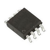
VO2631-X006 Vishay, VO2631-X006 Datasheet - Page 5

VO2631-X006
Manufacturer Part Number
VO2631-X006
Description
High Speed Optocouplers 10Mbd High-Speed Dual CTR>300%
Manufacturer
Vishay
Datasheet
1.6N137-X007T.pdf
(10 pages)
Specifications of VO2631-X006
Isolation Voltage
5300 Vrms
Maximum Continuous Output Current
50 mA
Maximum Fall Time
7 ns
Maximum Forward Diode Current
15 mA
Maximum Rise Time
23 ns
Minimum Forward Diode Voltage
1.1 V
Output Device
Logic Gate Photo IC
Configuration
2 Channel
Maximum Baud Rate
10 MBps
Maximum Forward Diode Voltage
1.7 V
Maximum Reverse Diode Voltage
5 V
Maximum Power Dissipation
60 mW
Maximum Operating Temperature
+ 100 C
Minimum Operating Temperature
- 40 C
Package / Case
PDIP-8
No. Of Channels
2
Optocoupler Output Type
Logic Gate
Input Current
10mA
Output Voltage
7V
Opto Case Style
DIP
No. Of Pins
8
Propagation Delay Low-high
49ns
Lead Free Status / RoHS Status
Lead free / RoHS Compliant
Note
• As per IEC 60747-5-5, §7.4.3.8.1, this optocoupler is suitable for “safe electrical insulation” only within the safety ratings. Compliance with
Document Number: 84732
Rev. 1.5, 08-Apr-11
THE PRODUCTS DESCRIBED HEREIN AND THIS DOCUMENT ARE SUBJECT TO SPECIFIC DISCLAIMERS, SET FORTH AT
SAFETY AND INSULATION RATINGS
PARAMETER
Climatic classification
Comparative tracking index
Peak transient overvoltage
Peak insulation voltage
Safety rating - power output
Safety rating - input current
Safety rating - temperature
Creepage distance
Clearance distance
Creepage distance
Clearance distance
Insulation thickness, reinforced rated
the safety ratings shall be ensured by means of prodective circuits.
I
F
V
FF
B
A
1
2
3
4
Single channel
Pulse generator
Z = 50 Ω
High Speed Optocoupler, Single and Dual,
O
Fig. 4 - Single Channel Test Circuit for Common Mode Transient Immunity
6N137, VO2601, VO2611, VO2630, VO2631, VO4661
Fig. 5 - Dual Channel Test Circuit for Common Mode Transient Immunity
+
18977-1
For technical questions, contact:
I
V
V
GND
F
-
CM
OUT
V
V
according to IEC 68 part 1
V
CC
FF
E
TEST CONDITION
B
A
8
6
5
This document is subject to change without notice.
7
Standard DIP-8
Standard DIP-8
per BSI 60950
400 mil DIP-8
400 mil DIP-8
V
CC
0.1 µF
bypass
1
2
3
4
10 MBd
Z
Pulse generator
Dual channel
O
R
+
L
Output V
monitoring
node
= 50 Ω
V
-
GND
CM
optocoupleranswers@vishay.com
V
O
CC
6
5
8
7
SYMBOL
V
V
CTI
P
IOTM
IORM
T
I
SO
SI
SI
V
0.1 µF
bypass
V
CM
O
V
O
0.5 V
0 V
5 V
R
V
L
CC
Switch AT A: I
Switch AT A:
Output V
monitoring
node
MIN.
8000
175
890
0.2
7
7
8
8
Vishay Semiconductors
O
55/100/21
I
F
F
V
TYP.
= 7.5 mA
= 0 mA
CM
V
V
O
O
(min.
(max.)
(PEAK)
www.vishay.com/doc?91000
)
MAX.
18976-2
399
500
300
175
www.vishay.com
CM
CM
H
L
UNIT
mW
mm
mm
mm
mm
mm
mA
°C
V
V
5


