EV31C3A3A1-27.000M Ecliptek, EV31C3A3A1-27.000M Datasheet

EV31C3A3A1-27.000M

Manufacturer Part Number
EV31C3A3A1-27.000M
Description
Manufacturer
Ecliptek
Datasheet

Specifications of EV31C3A3A1-27.000M

Output Frequency
27MHz
Symmetry Max
60%
Operating Supply Voltage (typ)
5
Mounting Style
Surface Mount
Screening Level
Commercial
Rad Hardened
No
Lead Free Status / RoHS Status
Compliant
ELECTRICAL SPECIFICATIONS
Nominal Frequency
Frequency Tolerance/Stability
Aging at 40°C
Operating Temperature Range
Supply Voltage
Input Current
Output Voltage Logic High (Voh)
Output Voltage Logic Low (Vol)
Rise/Fall Time
Duty Cycle
Load Drive Capability
Output Logic Type
Absolute Pull Range
Control Voltage
Control Voltage Range
Linearity
Transfer Function
Modulation Bandwidth
Input Impedance
Input Leakage Current
Phase Noise
Tri-State Input Voltage (Vih and Vil)
RMS Phase Jitter
Start Up Time
Storage Temperature Range
ENVIRONMENTAL & MECHANICAL SPECIFICATIONS
Fine Leak Test
Gross Leak Test
Mechanical Shock
Resistance to Soldering Heat
Resistance to Solvents
Solderability
Temperature Cycling
Vibration
EV31C3A3A1-27.000M
www.ecliptek.com | Specification Subject to Change Without Notice | Rev K 2/12/2011 | Page 1 of 6
Series
RoHS Compliant (Pb-free) 5.0V 6 Pad 5mm x 7mm
Ceramic SMD HCMOS/TTL VCXO (Tri-State Pad 5)
Operating Temperature Range
0°C to +70°C
27.000MHz
±50ppm Maximum (Inclusive of all conditions: Calibration Tolerance at 25°C, Frequency Stability over the
Operating Temperature Range, Supply Voltage Change, Output Load Change, Shock, and Vibration.)
±2ppm/First year typical, ±10ppm/10 Years Maximum
0°C to +70°C
5.0Vdc ±10%
25mA Maximum
90% of Vdd Minimum (IOH = -4mA)
10% of Vdd Maximum (IOL = +4mA)
5nSec Maximum (Measured at 0.4Vdc to 2.4Vdc with TTL Load; Measured at 20% to 80% of waveform
with HCMOS Load)
50 ±5(%) Typical, 50 ±10(%) Maximum (Measured at 1.4Vdc with TTL Load; Measured at 50% of
waveform with HCMOS Load)
10TTL Load or 30pF HCMOS Load Maximum
CMOS
±50ppm Minimum (Inclusive of all conditions: Calibration Tolerance at 25°C, Frequency Stability over the
Operating Temperature Range, Supply Voltage Change, Output Load Change, Shock, Vibration, and Aging
over the Control Voltage (Vc).)
0.5Vdc to 4.5Vdc (Test condition for Absolute Pull Range)
0.0Vdc to Vdd
10% Typical, 20% Maximum
Positive Transfer Characteristic
10kHz Minimum (Measured at -3dB, Vc = 2.5Vdc)
50kOhms Minimum
10µA Maximum
-70dBc/Hz at offset of 10Hz, -100dBc/Hz at offset of 100Hz, -130dBc/Hz at offset of 1kHz, -147dBc/Hz at
offset of 10kHz, -152dBc/Hz at offset of 100kHz, and -155dBc/Hz at offset of 1MHz (Typical Values at Fo =
27MHz)
+0.9Vdd Minimum to Enable Output; +0.1Vdd Maximum to Disable Output (High Impedance); No Connect
to Enable Output.
1pSec Maximum (Fj = 12kHz to 20MHz)
10mSec Maximum
-55°C to +125°C
MIL-STD-883, Method 1014 Condition A
MIL-STD-883, Method 1014 Condition C
MIL-STD-202, Method 213 Condition C
MIL-STD-202, Method 210
MIL-STD-202, Method 215
MIL-STD-883, Method 2003
MIL-STD-883, Method 1010
MIL-STD-883, Method 2007 Condition A
Absolute Pull Range
±50ppm Minimum
EV31C3 A 3 A 1 -27.000M
Linearity
10% Typical, 20% Maximum
Duty Cycle
50 ±5(%) Typical, 50 ±10(%) Maximum
RoHS
Nominal Frequency
27.000MHz
Pb

Related parts for EV31C3A3A1-27.000M

EV31C3A3A1-27.000M Summary of contents

Page 1

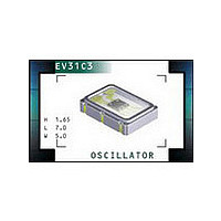
... EV31C3A3A1-27.000M Series RoHS Compliant (Pb-free) 5.0V 6 Pad 5mm x 7mm Ceramic SMD HCMOS/TTL VCXO (Tri-State Pad 5) Operating Temperature Range 0°C to +70°C ELECTRICAL SPECIFICATIONS Nominal Frequency 27.000MHz Frequency Tolerance/Stability ±50ppm Maximum (Inclusive of all conditions: Calibration Tolerance at 25°C, Frequency Stability over the Operating Temperature Range, Supply Voltage Change, Output Load Change, Shock, and Vibration.) Aging at 40° ...

Page 2

... EV31C3A3A1-27.000M MECHANICAL DIMENSIONS (all dimensions in millimeters) 5.00 1.65 ±0.15 ±0.20 Suggested Solder Pad Layout All Dimensions in Millimeters 1.8 (X6) 2.0 (X6) 0.54 (X4) Solder Land 1.89 (X6) All Tolerances are ±0.1 OUTPUT WAVEFORM V OH 80% or 2.4V DC 50% or 1.4V DC 20 Fall Time www.ecliptek.com | Specification Subject to Change Without Notice | Rev K 2/12/2011 | Page ...

Page 3

... EV31C3A3A1-27.000M Test Circuit for TTL Output Switch Power Supply Current Meter Power Voltage Supply Meter Power Voltage Supply Note 1: An external 0.1µF low frequency tantalum bypass capacitor in parallel with a 0.01µF high frequency ceramic bypass capacitor close to the package ground and V pin is required ...

Page 4

... EV31C3A3A1-27.000M Test Circuit for CMOS Output Switch Power Supply Power Voltage Supply Meter Power Supply Note 1: An external 0.1µF low frequency tantalum bypass capacitor in parallel with a 0.01µF high frequency ceramic bypass capacitor close to the package ground and V pin is required. ...

Page 5

... EV31C3A3A1-27.000M Recommended Solder Reflow Methods Max S T Min S High Temperature Infrared/Convection T MAX to T (Ramp-up Rate Preheat - Temperature Minimum (T MIN Temperature Typical (T TYP Temperature Maximum (T MAX Time (t MIN) S Ramp-up Rate ( Time Maintained Above: - Temperature ( Time ( Peak Temperature ( Target Peak Temperature (T Target) P Time within 5°C of actual peak (t ...

Page 6

... EV31C3A3A1-27.000M Recommended Solder Reflow Methods Max S T Min S Low Temperature Infrared/Convection 240°C T MAX to T (Ramp-up Rate Preheat - Temperature Minimum (T MIN Temperature Typical (T TYP Temperature Maximum (T MAX Time (t MIN) S Ramp-up Rate ( Time Maintained Above: - Temperature ( Time ( Peak Temperature ( Target Peak Temperature (T ...

Related keywords