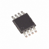
MAX2752EUA+ Maxim Integrated Products, MAX2752EUA+ Datasheet - Page 5

MAX2752EUA+
Manufacturer Part Number
MAX2752EUA+
Description
IC OSC VOLT CNTRL 8-UMAX
Manufacturer
Maxim Integrated Products
Series
MAX2752r
Type
Standardr
Datasheet
1.MAX2752EUAT.pdf
(6 pages)
Specifications of MAX2752EUA+
Function
VCO
Frequency
2.025GHz ~ 2.165GHz
Rf Type
ISM
Secondary Attributes
On-Chip Tank Circuit
Package / Case
8-MSOP, Micro8™, 8-uMAX, 8-uSOP,
Supply Voltage
2.7V ~ 5.5V
Operating Temperature
-40°C ~ 85°C
Supply Current
15.2mA
Lead Free Status / RoHS Status
Lead free / RoHS Compliant
Frequency Stability
-
Figure 1. Typical Application Circuit
The MAX2750/MAX2751/MAX2752 VCOs are imple-
mented as an LC oscillator topology, integrating all of
the tank components on-chip. This fully monolithic
approach provides an extremely easy-to-use VCO,
equivalent to a VCO module. The frequency is con-
trolled by a voltage applied to the TUNE pin, which is
internally connected to the varactor. The VCO core
uses a differential topology to provide a stable frequen-
cy versus supply voltage and improve the immunity to
load variations. In addition, there is a buffer amplifier
following the oscillator core to provide added isolation
from load variations and to boost the output power.
The oscillator signal from the core drives an output
buffer amplifier. The amplifier is internally matched to
50Ω including an on-chip DC blocking capacitor. No
external DC blocking capacitor is required, eliminating
the need for any external components. The output
amplifier has its own V
load-pulling effects. The amplifier boosts the oscillator
signal to a level suitable for driving most RF mixers.
SYNTHESIZER
FROM
SHDN
LOOP FILTER
_______________________________________________________________________________________
Detailed Description
0.1µF
CC
and GND pins to minimize
BYP
TUNE
GND
SHDN
Output Buffer
Oscillator
Voltage-Controlled Oscillators
OSCILLATOR
CORE
BIAS
The tuning input is typically connected to the output of
the PLL loop filter. The loop filter provides an appropri-
ately low-impedance source. The input may incorporate
an extra RC filter stage to reduce high-frequency noise
and spurious signals. Any excess noise on the tuning
input is directly translated into FM noise, which can
degrade the phase-noise performance of the oscillator.
Therefore, it is important to minimize the noise intro-
duced on the tuning input. A simple RC filter with low
corner frequency is needed during testing in order to
filter the noise present on the voltage source driving the
tuning line.
Always use controlled impedance lines (microstrip,
coplanar waveguide, etc.) for high-frequency signals.
Always place decoupling capacitors as close to the
V
essary to add additional decoupling capacitors located
further from the device. Always provide a low-induc-
tance path to ground, and keep GND vias as close to
the device as possible. Thermal reliefs on GND pads
are not recommended.
CC
pins as possible; for long V
MAX2750
MAX2751
MAX2752
2.4GHz Monolithic
V
V
GND
OUT
CC1
CC2
Applications Information
220pF
220pF
CC
lines, it may be nec-
Layout Issues
OUT TO MIXER/
SYNTHESIZER
Tune Input
V
CC
5


