NNDK-MOD5234LCKIT NetBurner Inc, NNDK-MOD5234LCKIT Datasheet - Page 3
NNDK-MOD5234LCKIT
Manufacturer Part Number
NNDK-MOD5234LCKIT
Description
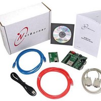
MCU, MPU & DSP Development Tools MOD5234 Core Module Development Kit
Manufacturer
NetBurner Inc
Datasheet
1.MOD5234-100IR.pdf
(4 pages)
Specifications of NNDK-MOD5234LCKIT
Processor To Be Evaluated
MOD5234
Interface Type
RS-232
Lead Free Status / RoHS Status
Lead free / RoHS Compliant


MOD5234 Pinout and Signal Description
The MOD5234 module has two dual in-line 50 pin headers which enable you to quickly and easily connect to one of our standard
NetBurner Carrier Boards, or a board you create on your own. Table 2 provides descriptions of pin function of the MOD5234 header.
Table 2: NetBurner MOD5234 Pinout and Signal Descriptions
Note:
1. Asterisk (*) denotes active low. All input/output lines are 3.3V only.
2. The TIP signal is the logical AND of *CS1, *CS2 and *CS3. TIP can used to
control an external data bus buffer for the data bus signals. An example
circuit design can be found on the Module Development Board schematic.
An external data bus buffer is recommended for any designs that use data
bus signals D16 - D31.
Pin
10
11
12
13
14
15
16
17
18
19
20
21
22
23
24
25
26
27
28
29
30
31
32
33
34
35
36
37
38
39
40
41
42
43
44
45
46
47
48
49
50
1
2
3
4
5
6
7
8
9
CLK_OUT³
Function
e t B u r n e r
VCC3V
VCC3V
*RSTO
*CS1¹
*CS2¹
*CS3¹
R/*W
*RSTI
GND
GND
*BS2
*BS3
GND
GND
*TIP
D16
D18
D17
D20
D19
D22
D21
D24
D23
D26
D25
D28
D27
D30
D29
D31
A10
A11
A12
A13
A14
A15
*OE
*TA
Networking in 1 Day!
A0
A1
A2
A3
A4
A5
A6
A7
A8
A9
GPIO Port
PBUSCTL6
PCS1
PCS2
PCS3
J1 Connector
Description
Ground
Ground
Input power 3.3 VDC
Data Bus - Read / NOT Write
Data Bus - Chip Select 1
Data Bus - Chip Select 2
Data Bus - Chip Select 3
Data Bus - Output Enable
Byte Strobe for D16 to D23 (8 bits)
Byte Strobe for D24 to D31 (8 bits)
Data Bus - Transfer in Progress
Data Bus - Data 16
Data Bus - Transfer Acknowledge
Data Bus - Data 18
Data Bus - Data 17
Data Bus - Data 20
Data Bus - Data 19
Data Bus - Data 22
Data Bus - Data 21
Data Bus - Data 24
Data Bus - Data 23
Data Bus - Data 26
Data Bus - Data 25
Data Bus - Data 28
Data Bus - Data 27
Data Bus - Data 30
Data Bus - Data 29
Processor Reset Input
Data Bus - Data 31
Processor Reset Output
Buffer Clock Out (CLKOUT-73.728 Mhz)
Data Bus - Address 0
Data Bus - Address 1
Data Bus - Address 2
Data Bus - Address 3
Data Bus - Address 4
Data Bus - Address 5
Data Bus - Address 6
Data Bus - Address 7
Data Bus - Address 8
Data Bus - Address 9
Data Bus - Address 10
Data Bus - Address 11
Data Bus - Address 12
Data Bus - Address 13
Data Bus - Address 14
Data Bus - Address 15
Input power 3.3 VDC
Ground
Ground
2
3
3. The CLKOUT signal is 1/2 the system frequency of 147.456 MHz.
4. Each UART can be clocked from an internal or external source. For external clocks,
each UARTn,can be clocked by the corresponding DTn_IN input pin.
5. If using I2C, the module must add pull-up resistors to SDA/SCL.
6. Plus sign (+) denotes additional alternate pin function
Pin
10
11
12
13
14
15
16
17
18
19
20
21
22
23
24
25
26
27
28
29
30
31
32
33
34
35
36
37
38
39
40
41
42
43
44
45
46
47
48
49
50
+
1
2
3
4
5
6
7
8
9
6
(1)
QSPI_DOUT
UTPUODIS
*QSPI_CS1
LTPUODIS
Function
TPUCH11
TPUCH10
TPUCH13
TPUCH12
TPUCH15
TPUCH14
QSPI_CLK
QSPI_DIN
QSPI_CS0
*U0_CTS
DT2OUT
DT1OUT
DT0OUT
*U0_RTS
I2C_SDA
U0_RXD
U0_TXD
TPUCH1
TPUCH0
TPUCH3
TPUCH2
TPUCH5
TPUCH4
TPUCH7
TPUCH6
TPUCH9
TPUCH8
U1_RXD
U1_TXD
U2_RXD
I2C_SCL
U2_TXD
*U1CTS
TCRCLK
*U1RTS
DT0_IN
DT1_IN
VCC3V
VCC3V
*IRQ1
*IRQ3
*IRQ5
*IRQ7
GND
GND
GND
Alt. Func.
DT1_OUT
CAN0RX
CAN0TX
I2C_SDA
CAN0RX
CAN0TX
I2C_SCL
*DREQ0
*DREQ1
*U2CTS
SD_CKE
*U2RTS
DACK2
DACK1
DACK0
GPIO Port
PFEC12C1
PUARTH0
PUARTH1
PETUPU2
PFECI2C0
PUARTL0
PUARTL1
PUARTL4
PUARTL5
PUARTL6
PUARTL7
PUARTL3
PUARTL2
PTIMER1
PTIMER4
PTIMER2
PTIMER0
PTIMER3
ETPU11
ETPU10
ETPU13
ETPU12
ETPU15
ETPU14
PETPU1
PETPU0
PQSPI2
PQSPI1
PQSPI0
PQSPI3
PQSPI4
ETPU1
ETPU0
ETPU3
ETPU2
ETPU5
ETPU4
ETPU7
ETPU6
ETPU9
ETPU8
PIRQ1
PIRQ3
PIRQ5
PIRQ7
J2 Connector
Description
Ground
Input power 3.3 VDC
Data Bus - UART 0 Receive
Data Bus - UART 0 Transmit
eTPU Channel 1
eTPU Channel 0
eTPU Channel 3
eTPU Channel 2
eTPU Channel 5
eTPU Channel 4
eTPU Channel 7
eTPU Channel 6
eTPU Channel 9
eTPU Channel 8
eTPU Channel 11
eTPU Channel 10
eTPU Channel 13
eTPU Channel 12
eTPU Channel 15
eTPU Channel 14
Data Bus - UART 1 Receive
Data Bus - UART 1
Data Bus - UART 1
Data Bus - UART 1
QSPI Clock or I
Clock the TCR counters or gate the TCR2 clock
QSPI Input or I
QSPI Data Out
UART0 Clear To Send
QSPI Chip Select 0
DMA Timer 0 In or DMA Request 0
eTPU Channel Output Disable Signal (Upper)
DMA Timer 2 Out or DMA Acknowledge 2
DMA Timer 1 Out or DMA Acknowledge 1
eTPU Channel Output Disable Signal (Lower)
DMA Timer 0 Out or Acknowledge 0
DMA Timer 1 In or DMA Timer 1 Out
DMA Request 1
Data Bus - UART 0 Request To Send
Data Bus - I
QSPI Chip Select 1 or SDRAM Clock Enable
Data Bus - UART 2 Receive
Data Bus - I
External Interrupt 1
Data Bus - UART 2 Transmit
External Interrupt 3
Ground
External Interrupt 5
External Interrupt 7
Ground
Input power 3.3 VDC
2
2
C Data Line
C Clock Line
2
2
C Data Line
C Clock
MOD5234
4
4
or UART 2 Request to Send
4
or UART 2 Clear to Send
or CAN 0 Transmit
4
5
5
or CAN 0 Receive
5
or CAN 0 Transmit
4
4
4
5
4
or CAN 0 Receive
4
6
4
4
4
Related parts for NNDK-MOD5234LCKIT
Image
Part Number
Description
Manufacturer
Datasheet
Request
R

Part Number:
Description:
BOARD SERIAL-ETHERNET 512K FLASH
Manufacturer:
NetBurner Inc
Datasheet:

Part Number:
Description:
PROCESSOR MODULE FLASH MOD5272
Manufacturer:
NetBurner Inc
Datasheet:

Part Number:
Description:
PROCESSOR MODULE 512KB FLASH
Manufacturer:
NetBurner Inc
Datasheet:

Part Number:
Description:
DUAL PORT SERIAL-ETHERNET
Manufacturer:
NetBurner Inc
Datasheet:

Part Number:
Description:
PROCESSOR MODULE FLASH
Manufacturer:
NetBurner Inc
Datasheet:

Part Number:
Description:
PROCESSOR MODULE 512KB FLASH
Manufacturer:
NetBurner Inc
Datasheet:

Part Number:
Description:
MOD5234 10/100 ETHERNET MODULE
Manufacturer:
NetBurner Inc
Datasheet:

Part Number:
Description:
KIT DEVELOP NETWORK FOR MOD5282
Manufacturer:
NetBurner Inc
Datasheet:

Part Number:
Description:
KIT DEVELOP NETWORK FOR MOD5272
Manufacturer:
NetBurner Inc
Datasheet:

Part Number:
Description:
DUAL PORT SERIAL-ETHERNET
Manufacturer:
NetBurner Inc
Datasheet:

Part Number:
Description:
Ethernet Modules & Development Tools 32 Bit 66MHz 40 Pin DIP Industrial Temp
Manufacturer:
NetBurner Inc
Datasheet:

Part Number:
Description:
Ethernet Modules & Development Tools MOD5213 DEVELOPMENT KIT
Manufacturer:
NetBurner Inc

Part Number:
Description:
Ethernet ICs 32bit 147MHz CAN-to- Ethnt Device IndTemp
Manufacturer:
NetBurner Inc
Datasheet: