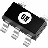
NCP4625DSN12T1G ON Semiconductor, NCP4625DSN12T1G Datasheet

NCP4625DSN12T1G
Specifications of NCP4625DSN12T1G
Available stocks
Related parts for NCP4625DSN12T1G
NCP4625DSN12T1G Summary of contents
Page 1
NCP4625 300 mA Low Dropout Regulator The NCP4625 is a CMOS Linear voltage regulator with 300 mA output current capability. The device is capable of operating with input voltages with high output voltage accuracy ...
Page 2
VIN Vref Current Limit Thermal Shutdown CE NCP4625Hxxxx Figure 2. Simplified Schematic Block Diagram PIN FUNCTION DESCRIPTION Pin No. Pin No. Pin No. SOT89 SC−70 SOT23 ...
Page 3
THERMAL CHARACTERISTICS Rating Thermal Characteristics, SOT89 Thermal Resistance, Junction−to−Air Thermal Characteristics, SOT23 Thermal Resistance, Junction−to−Air Thermal Characteristics, SC−70 Thermal Resistance, Junction−to−Air ELECTRICAL CHARACTERISTICS −40°C ≤ T otherwise noted. Typical values are +25°C. A Parameter Operating Input Voltage ...
Page 4
0.8 0.6 0.4 0.2 0.0 0 100 200 300 I (mA) OUT Figure 3. Output Voltage vs. Output Current 1.2 V Version (T = 255C) J 6.0 5 5.3 V ...
Page 5
T , JUNCTION TEMPERATURE (°C) J Figure 9. Output Voltage vs. Temperature, 1.2 V Version 5.10 5.08 5.06 5.04 5.02 5.00 4.98 4.96 4.94 ...
Page 6
I = 200 mA OUT 1.0 0.5 0 INPUT VOLTAGE (V) IN Figure 15. Output Voltage vs. Input Voltage, 2.8 V Version ...
Page 7
I = 100 mA OUT 0.01 0 FREQUENCY (kHz) Figure 21. PSRR, 5.0 V Version, V 3.0 2.5 2.0 1.5 1.0 0.5 0.0 0.01 0.1 ...
Page 8
TYPICAL CHARACTERISTICS 1.220 1.215 1.210 1.205 1.200 1.195 1.190 (ms) Figure 26. Line Transients, 1.2 V Version ms OUT 2.820 2.815 ...
Page 9
TYPICAL CHARACTERISTICS 1.24 1.22 1.20 1.18 1.16 1. 100 120 140 160 180 200 t (ms) Figure 29. Load Transients, 1.2 V Version – 100 mA 0.5 ms, ...
Page 10
TYPICAL CHARACTERISTICS 1.40 1.30 1.20 1.10 1.00 0. 100 150 200 250 300 350 400 450 500 t (ms) Figure 32. Load Transients, 1.2 V Version – 150 mA 0.5 ms, ...
Page 11
TYPICAL CHARACTERISTICS Chip Enable 2.0 1 OUT 1 300 mA OUT I 0.5 OUT 0.0 −0 100 120 140 160 180 200 t (ms) Figure 35. Start−up, 1.2 V ...
Page 12
TYPICAL CHARACTERISTICS Chip Enable 2 OUT 1.5 1 OUT 0.5 0 300 mA OUT −0.5 0.0 0.2 0.4 0.6 0.8 1.0 1.2 t (ms) Figure 38. Shutdown, 1.2 V Version ...
Page 13
A typical application circuit for NCP4625 series is shown in Figure 41. NCP4625x VIN VIN VOUT GND Figure 41. Typical Application Schematic Input Decoupling Capacitor (C1 ceramic input decoupling capacitor should be connected as ...
Page 14
... ORDERING INFORMATION Nominal Output Voltage Device NCP4625DSN12T1G 1.2 V NCP4625DSN18T1G 1.8 V NCP4625DSN28T1G 2.8 V NCP4625DSN30T1G 3.0 V NCP4625DSN33T1G 3.3 V NCP4625DSN50T1G 5.0 V NCP4625HSN12T1G 1.2 V NCP4625HSN18T1G 1.8 V NCP4625HSN28T1G 2.8 V NCP4625HSN30T1G 3.0 V NCP4625HSN33T1G 3.3 V NCP4625HSN50T1G 5.0 V †For information on tape and reel specifications, including part orientation and tape sizes, please refer to our Tape and Reel Packaging Specifications Brochure, BRD8011/D ...
Page 15
SC−88A (SC−70−5/SOT−353 −B− 0.2 (0.008 PACKAGE DIMENSIONS CASE 419A−02 ISSUE K NOTES: 1. DIMENSIONING AND TOLERANCING PER ANSI Y14.5M, 1982. 2. CONTROLLING DIMENSION: INCH. 3. ...
Page 16
... RECOMMENDED MOUNTING FOOTPRINT* 0.57 4X 0.45 2.79 1.30 1 1.50 2X DIMENSIONS: MILLIMETERS *For additional information on our Pb−Free strategy and soldering details, please download the ON Semiconductor Soldering and Mounting Techniques Reference Manual, SOLDERRM/D. http://onsemi.com 16 MILLIMETERS MIN MAX 1.40 1.60 0.32 0.52 0.37 0.57 ...
Page 17
... Opportunity/Affirmative Action Employer. This literature is subject to all applicable copyright laws and is not for resale in any manner. PUBLICATION ORDERING INFORMATION LITERATURE FULFILLMENT: Literature Distribution Center for ON Semiconductor P.O. Box 5163, Denver, Colorado 80217 USA Phone: 303−675−2175 or 800−344−3860 Toll Free USA/Canada Fax: 303− ...


