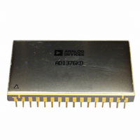
AD1376JD Analog Devices Inc, AD1376JD Datasheet - Page 7

AD1376JD
Manufacturer Part Number
AD1376JD
Description
A/D Converter (A-D) IC
Manufacturer
Analog Devices Inc
Datasheet
1.AD1376JD.pdf
(12 pages)
Specifications of AD1376JD
No. Of Bits
16 Bit
Mounting Type
Through Hole
Interface Type
Serial, Parallel
Package / Case
32-DIP
Rohs Status
RoHS non-compliant
Number Of Bits
16
Sampling Rate (per Second)
62.5k
Data Interface
Parallel
Number Of Converters
1
Power Dissipation (max)
800mW
Voltage Supply Source
Dual ±
Operating Temperature
0°C ~ 70°C
Lead Free Status / RoHS Status
Available stocks
Company
Part Number
Manufacturer
Quantity
Price
INTERNAL
In either adjustment circuit, the fixed resistor connected to
Pin 27 should be located close to this pin to keep the pin
connection short. Pin 27 is quite sensitive to external noise
pickup and should be guarded by ANALOG COMMON.
TIMING
The timing diagram is shown in Figure 8. Receipt of a
CONVERT START signal sets the STATUS flag, indicating
conversion in progress. This in turn removes the inhibit applied
to the gated clock, permitting it to run through 17 cycles. All
the SAR parallel bits, the STATUS flip-flops, and the gated clock
inhibit signal are initialized on the trailing edge of the
CONVERT START signal. At time t
set unconditionally. At t
Bit 2 is reset unconditionally. This sequence continues until the
Bit 16 (LSB) decision (keep) is made at t
reset, indicating that the conversion is complete and that the
parallel output data is valid. Resetting the STATUS flag restores
the gated clock inhibit signal, forcing the clock output to the
low Logic 0 state. Note that the clock remains low until the next
conversion.
Corresponding parallel data bits become valid on the same
positive-going clock edge.
CONVERT
STATUS
CLOCK
START
BIT 10
BIT 11
BIT 12
BIT 13
BIT 14
BIT 15
BIT 2
BIT 3
BIT 4
BIT 5
BIT 6
BIT 7
BIT 8
BIT 9
MSB
LSB
NOTES:
1. THE CONVERT START PULSEWIDTH IS 50ns MIN AND MUST REMAIN LOW DURING A
2. MSB DECISION.
3. CLOCK REMAINS LOW AFTER LAST BIT DECISION.
(1)
CONVERSION. THE CONVERSION IS INITIATED BY THE TRAILING EDGE OF THE
CONVERT COMMAND.
Figure 8. Timing Diagram (Binary Code 0110011101111010)
t
0
0
MSB
(2)
t
0
1
t
1
1
2
t
1
1
3
t
0
0
4
1
t
MAXIMUM THROUGHPUT TIME
0
0
5
, the Bit 1 decision is made (keep) and
CONVERSION TIME (2)
t
1
1
6
t
1
1
7
t
1
1
8
t
0
0
9
0
, B
t
10
1
1
1
16
t
is reset and B
11
1
1
. The STATUS flag is
t
12
1
1
t
13
1
1
t
14
0
0
t
15
1
1
2
t
(3)
–B
0
0
16
t
17
16
are
LSB
Rev. D | Page 7 of 12
DIGITAL OUTPUT DATA
Parallel data from TTL storage registers is in negative true form
(Logic 1 = 0 V and Logic 0 = 2.4 V). Parallel data output coding
is complementary binary for unipolar ranges and complement-
tary offset binary for bipolar ranges. Parallel data becomes valid
at least 20 ns before the STATUS flag returns to Logic 0,
permitting parallel data transfer to be clocked on the 1 to 0
transition of the STATUS flag (see Figure 9). Parallel data
output changes state on positive going clock edges.
Short Cycle Input
Pin 32 (SHORT CYCLE) permits the timing cycle shown in
Figure 8 to be terminated after any number of desired bits has
been converted, allowing somewhat shorter conversion times in
applications not requiring full 16-bit resolution. When 10-bit
resolution is desired, Pin 32 is connected to Bit 11 output
Pin 11. The conversion cycle then terminates and the STATUS
flag resets after the Bit 10 decision (Figure 8). Short cycle
connections and associated 8-, 10-, 12-, 13-, 14-, and 15-bit
conversion times are summarized in Table 3 for a 1.6 MHz
clock (AD1377) or 933 kHz clock (AD1376).
Table 3. Short Cycle Connections
Bits
16
15
14
13
12
10
8
INPUT SCALING
The ADC inputs should be scaled as close to the maximum
input signal range as possible to use the maximum signal
resolution of the ADC. Connect the input signal as shown in
Table 4. See Figure 10 for circuit details.
Resolution
(%
FSR)
0.0015 10
0.003
0.006
0.012
0.024
0.100
0.390
(STATUS)
BIT 16
VALID
BUSY
Maximum
Conversion Time (µs)
AD1377
9.4
8.7
8.1
7.5
6.3
5.0
Figure 9. LSB Valid to Status Low
AD1376
17.1
16.1
15.0
13.9
12.9
10.7
8.6
20ns MIN TO 90ns
Status
Flag
Reset
t
t
t
t
t
t
t
16
15
1
13
12
10
8
AD1376/AD1377
Connect
Short Cycle
Pin 32 to
NC (Open)
Pin 16
Pin 15
Pin 14
Pin 13
Pin 11
Pin 9


