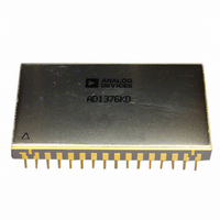
AD1380JD Analog Devices Inc, AD1380JD Datasheet - Page 8

AD1380JD
Manufacturer Part Number
AD1380JD
Description
IC,A/D CONVERTER,SINGLE,16-BIT,HYBRID,DIP,32PIN
Manufacturer
Analog Devices Inc
Datasheet
1.AD1380JD.pdf
(12 pages)
Specifications of AD1380JD
Rohs Status
RoHS non-compliant
Number Of Bits
16
Sampling Rate (per Second)
50k
Data Interface
Parallel
Number Of Converters
1
Power Dissipation (max)
900mW
Voltage Supply Source
Dual ±
Operating Temperature
0°C ~ 70°C
Mounting Type
Through Hole
Package / Case
32-DIP (0.900", 22.86)
Lead Free Status / RoHS Status
AD1380
DIGITAL OUTPUT DATA
Parallel data from TTL storage registers is in negative true form
(Logic 1 = 0 V and Logic 0 = 2.4 V). Parallel data output coding
is complementary binary for unipolar ranges and comple-
mentary offset binary for bipolar ranges. Parallel data becomes
valid at least 20 ns before the STATUS flag returns to Logic 0,
permitting parallel data transfer to be clocked on the 1 to 0
transition of the STATUS flag (see
output changes state on positive going clock edges.
Table 3. Input Scaling Connections
Input Signal Line
±10 V
±5 V
±2.5 V
0 V to +5 V
0 V to +10 V
1
Table 4. Transition Values vs. Calibration Codes
Output Code
MSB
000. . . .000
011 . . . 111
111 . . . 110
1
2
Table 5. Input Voltage Range and LSB Values
Analog Input Voltage Range
Code Designation
One Least Significant Bit (LSB)
1
2
3
Pin 5 is extremely sensitive to noise and should be guarded by ANALOG COMMON.
For LSB value for range and resolution used, see Table 5.
Voltages given are the nominal value for transition to the code specified.
COB = complementary offset binary.
CTC = complementary twos complement—achieved by using an inverter to complement the most significant bit to produce MSB .
CSB = complementary straight binary.
LSB
(STATUS)
2
BIT 16
VALID
1
BUSY
Figure 7. LSB Valid to Status Low
Output Code
COB
COB
COB
CSB
CSB
Range
+Full Scale
Midscale
−Full Scale
20ns MIN TO 90ns
Figure 7). Parallel data
n = 8
n = 10
n = 12
n = 13
n = 14
n = 15
FSR
2
n
±10 V
+10 V
−3/2 LSB
0 V
−1/2 LSB
−10 V
+1/2 LSB
Connect Pin 4 to
Pin 5
Pin 5
Pin 5
Open
Open
±10 V
COB or CTC
78.13 mV
19.53 mV
4.88 mV
2.44 mV
1.22 mV
0.61 mV
20
2
1
1
1
n
V
1
Rev. D | Page 8 of 12
2
±5 V
+5 V
−3/2 LSB
0 V
−1/2 LSB
−5 V
+1/2 LSB
±5 V
COB
39.06 mV
9.77 mV
2.44 mV
1.22 mV
0.61 mV
0.31 mV
10
2
Connect Pin 7 to
Pin 32
Open
Pin 5
Pin 5
Open
n
V
1
or CTC
INPUT SCALING
The AD1380 inputs should be scaled as close to the maximum
input signal range as possible to use the maximum signal
resolution of the ADC. Connect the input signal as shown in
Table 3. See Figure 8 for circuit details.
1
1
±2.5 V
−3/2 LSB
−1/2 LSB
+1/2 LSB
COMPARATOR
+2.5 V
0 V
−2.5 V
2
COMMON
BIPOLAR
ANALOG
OFFSET
±2.5 V
COB
19.53 mV
4.88 mV
1.22 mV
0.61 mV
0.31 mV
0.15 mV
5
2
V
n
IN
1
or CTC
6
7
5
4
8
Figure 8. Input Scaling Circuit
Connect Input
Signal to
Pin 31
Pin 31
Pin 31
Pin 31
Pin 31
10V SPAN
20V SPAN
0 V to +10 V
+10 V
−3/2 LSB
+5 V
−1/2 LSB
0 V
+1/2 LSB
3.75kΩ
FROM DAC
7.5kΩ
2
R2
0 V to +10 V
CSB
39.06 mV
9.77 mV
2.44 mV
1.22 mV
0.61 mV
0.31 mV
10
2
n
R1
3.75kΩ
3
V
V
REF
COMPARATOR
Connect Pin 32 to
Pin 7
Pin 6
Pin 6
Pin 6
Pin 6
0 V to +5 V
+5 V
−3/2 LSB
+2.5 V
−1/2 LSB
0 V
+1/2 LSB
0 V to +5 V
CSB
19.53 mV
4.88 mV
1.22 mV
0.61 mV
0.31 mV
0.15 mV
5
2
V
n
3
TO
SAR


