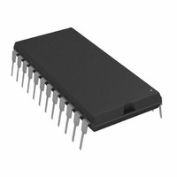
AD1865N-K Analog Devices Inc, AD1865N-K Datasheet - Page 3

AD1865N-K
Manufacturer Part Number
AD1865N-K
Description
IC, DUAL 18-BIT AUDIO DAC
Manufacturer
Analog Devices Inc
Datasheet
1.AD1865N-J.pdf
(12 pages)
Specifications of AD1865N-K
Rohs Status
RoHS non-compliant
Number Of Bits
18
Data Interface
Serial
Number Of Converters
2
Voltage Supply Source
Analog and Digital, Dual ±
Power Dissipation (max)
260mW
Operating Temperature
-25°C ~ 70°C
Mounting Type
Through Hole
Package / Case
24-DIP (0.600", 15.24mm)
Settling Time
-
Lead Free Status / RoHS Status
Available stocks
Company
Part Number
Manufacturer
Quantity
Price
REV. 0
CAUTION
ESD (electrostatic discharge) sensitive device. Electrostatic charges as high as 4000 V readily
accumulate on the human body and test equipment and can discharge without detection.
Although the AD1865 features proprietary ESD protection circuitry, permanent damage may
occur on devices subjected to high energy electrostatic discharges. Therefore, proper ESD
precautions are recommended to avoid performance degradation or loss of functionality.
ABSOLUTE MAXIMUM RATINGS*
V
V
–V
AGND to DGND . . . . . . . . . . . . . . . . . . . . . . . . . . . .
Digital Inputs to DGND . . . . . . . . . . . . . . . . . . . . . –0.3 to V
Short Circuit Protection . . . . . . . . Indefinite Short to Ground
Soldering (10 sec) . . . . . . . . . . . . . . . . . . . . . . . . . . . +300 C
Model
AD1865N
AD1865N-J
AD1865R
AD1865R-J
*N = Plastic DIP, R = Small Outline IC Package.
DIP SOIC
11
12
13
14
15
16
17
18
19
10
11
12
13
14
15
16
17
18
19
20
21
22
23
24
*Pin 16 has no internal connection; –V
applied.
L
S
S
to DGND . . . . . . . . . . . . . . . . . . . . . . . . . . . . 0 V to 6.0 V
to AGND . . . . . . . . . . . . . . . . . . . . . . . . . . . . 0 V to 6.0 V
to AGND . . . . . . . . . . . . . . . . . . . . . . . . . . –6.0 V to 0 V
22
23
24
26
28
11
12
13
14
15
16
17
18
19
10
11, 16, 18 NC
25, 27
12
13
14
15
17
19
20
21
–V
TRIM Right Channel Trim Network Connection
MSB
I
AGND Analog Common Pin
SJ
R
V
+V
DR
LR
CLK
DGND Digital Common Pin
LL
DL
V
R
SJ
AGND Analog Common Pin
I
MSB
TRIM Left Channel Trim Network Connection
+V
Temperature
Range
–25 C to +70 C
–25 C to +70 C
–25 C to +70 C
–25 C to +70 C
OUT
OUT
OUT
OUT
F
F
S
L
S
PIN DESIGNATIONS
ORDERING GUIDE
Negative Analog Supply
Right Channel Trim Potentiometer
Wiper Connection
Right Channel Output Current
Right Channel Amplifier Summing Junction
Right Channel Feedback Resistor
Right Channel Output Voltage
Positive Digital Supply
Right Channel Data Input Pin
Right Channel Latch Pin
Clock Input Pin
Left Channel Latch Pin
Left Channel Data Input Pin
No Internal Connection*
Left Channel Output Voltage
Left Channel Feedback Resistor
Left Channel Amplifier Summing Junction
Left Channel Output Current
Left Channel Trim Potentiometer
Wiper Connection
Positive Analog Supply
L
from AD1864 DIP socket can be safely
THD+N @ FS
0.006%
0.004%
0.006%
0.004%
Package
Option*
N-24A
N-24A
R-28
R-28
0.3 V
L
–3–
*Stresses greater than those listed under “Absolute Maximum Ratings” may cause
permanent damage to the device. This is a stress rating only and functional
operation of the device at these or any other conditions above those indicated in the
operational section of this specification is not implied. Exposure to absolute
maximum rating conditions for extended periods may affect device reliability.
CHANNEL
RIGHT
AGND
TRIM
V
MSB
I
+V
CLK
–V
OUT
OUT
DR
R
LR
DGND
SJ
V
F
L
S
+V
V
(24-Pin DIP Package)
OUT
CLK
OUT
DR
NC
LR
DL
(28-Pin SOIC Package)
R
R
SJ
SJ
LL
L
F
F
10
12
11
4
6
7
8
9
1
2
3
5
10
12
13
14
11
1
4
5
7
2
3
6
8
9
NC = NO CONNECT
(Not to Scale)
PINOUT
NC = NO CONNECT
AD1865
TOP VIEW
(Not to Scale)
AD1865
TOP VIEW
WARNING!
24
23
22
21
20
19
18
17
16
15
14
13
28
22
25
24
21
19
18
17
16
15
27
26
23
20
+V
TRIM
R
NC
DL
DGND
ESD SENSITIVE DEVICE
MSB
V
LL
I
AGND
SJ
OUT
F
OUT
S
–V
AGND
TRIM
AGND
NC
I
+V
TRIM
MSB
I
NC
MSB
NC
OUT
NC
OUT
AD1865
S
S
LEFT
CHANNEL


