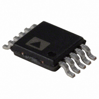
AD5172BRM10-RL7 Analog Devices Inc, AD5172BRM10-RL7 Datasheet - Page 6

AD5172BRM10-RL7
Manufacturer Part Number
AD5172BRM10-RL7
Description
IC,Digital Potentiometer,TSSOP,10PIN,PLASTIC
Manufacturer
Analog Devices Inc
Datasheet
1.AD5172BRMZ2.5.pdf
(24 pages)
Specifications of AD5172BRM10-RL7
Rohs Status
RoHS non-compliant
Taps
256
Resistance (ohms)
10K
Number Of Circuits
2
Temperature Coefficient
35 ppm/°C Typical
Memory Type
Non-Volatile
Interface
I²C, 2-Wire Serial
Voltage - Supply
2.7 V ~ 5.5 V
Operating Temperature
-40°C ~ 125°C
Mounting Type
Surface Mount
Package / Case
10-MSOP, Micro10™, 10-uMAX, 10-uSOP
Resistance In Ohms
10K
Lead Free Status / RoHS Status
AD5172/AD5173
TIMING CHARACTERISTICS
V
Table 3.
Parameter
I
1
2
Timing Diagram
2
See the timing diagrams for the locations of measured values (that is, see Figure 3 and Figure 48 to Figure 51).
The maximum t
C INTERFACE TIMING CHARACTERISTICS
DD
SCL Clock Frequency
Bus-Free Time Between Stop and Start, t
Hold Time (Repeated Start), t
Low Period of SCL Clock, t
High Period of SCL Clock, t
Setup Time for Repeated Start Condition, t
Data Hold Time, t
Data Setup Time, t
Fall Time of Both SDA and SCL Signals, t
Rise Time of Both SDA and SCL Signals, t
Setup Time for Stop Condition, t
OTP Program Time
= 5 V ± 10%, or 3 V ± 10%; V
SDA
SCL
HD;DAT
P
has to be met only if the device does not stretch the low period (t
HD;DAT
SU;DAT
t
1
2
S
LOW
HIGH
t
2
HD;STA
A
SU;STO
= V
t
3
DD
1
F
; V
BUF
R
t
8
SU;STA
B
t
8
= 0 V; −40°C < T
t
Figure 3. I
9
t
6
2
C Interface Detailed Timing Diagram
Symbol
f
t
t
t
t
t
t
t
t
t
t
t
SCL
1
2
3
4
5
6
7
8
9
10
11
t
t
4
Rev. H | Page 6 of 24
9
A
< +125°C; unless otherwise noted.
Conditions
After this period, the first clock
pulse is generated.
LOW
t
7
) of the SCL signal.
S
t
5
t
2
Min
1.3
0.6
1.3
0.6
0.6
100
0.6
Typ
400
P
Max
400
0.9
300
300
t
10
Unit
kHz
μs
μs
μs
μs
μs
μs
ns
ns
ns
μs
ms


