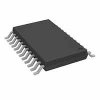
AD5206BRU10 Analog Devices Inc, AD5206BRU10 Datasheet - Page 4

AD5206BRU10
Manufacturer Part Number
AD5206BRU10
Description
Digital Potentiometer IC Package/Case:24-TSSOP
Manufacturer
Analog Devices Inc
Datasheet
1.AD5204BRUZ50.pdf
(20 pages)
Specifications of AD5206BRU10
Leaded Process Compatible
No
Peak Reflow Compatible (260 C)
No
Rohs Status
RoHS non-compliant
Taps
256
Resistance (ohms)
10K
Number Of Circuits
6
Temperature Coefficient
700 ppm/°C Typical
Memory Type
Volatile
Interface
SPI, 3-Wire Serial
Voltage - Supply
2.7 V ~ 5.5 V, ±2.3 V ~ 2.7 V
Operating Temperature
-40°C ~ 85°C
Mounting Type
Surface Mount
Package / Case
24-TSSOP
Resistance In Ohms
10K
Lead Free Status / RoHS Status
Contains lead / RoHS non-compliant
Available stocks
Company
Part Number
Manufacturer
Quantity
Price
Part Number:
AD5206BRU10
Manufacturer:
ADI/亚德诺
Quantity:
20 000
AD5204/AD5206
Parameter
INTERFACE TIMING CHARACTERISTICS
1
2
3
4
5
6
7
8
9
10
11
12
13
Typicals represent average readings at 25°C and V
Applies to all VRs.
Resistor position nonlinearity error (R-INL) is the deviation from an ideal value measured between the maximum resistance and the minimum resistance wiper positions.
R-DNL measures the relative step change from the ideal position between successive tap positions. Parts are guaranteed monotonic. See the test circuit in Figure 28.
I
V
INL and DNL are measured at V
of ±1 LSB maximum are guaranteed monotonic at operating conditions. See the test circuit in Figure 27.
Resistor Terminal A, Terminal B, and Wiper W have no limitations on polarity with respect to each other.
Guaranteed by design and not subject to production test.
Measured at the Ax terminals. All Ax terminals are open circuited in shutdown mode.
P
W
and timed from a voltage level of 1.5 V. Switching characteristics are measured using both V
All dynamic characteristics use V
Applies to all parts.
See the timing diagrams (Figure 3 to Figure 5) for the location of the measured values. All input control voltages are specified with t
The propagation delay depends on the values of V
AB
DISS
Input Clock Pulse Width
Data Setup Time
Data Hold Time
CLK-to-SDO Propagation Delay
CS Setup Time
CS High Pulse Width
Reset Pulse Width
CLK Fall to CS Fall Setup
CLK Fall to CS Rise Hold Time
CS Rise to Clock Rise Setup
= V
= V
is calculated from (I
DD
DD
/R for both V
, wiper (V
W
) = no connect.
DD
= 3 V and V
DD
× V
DD
W
). CMOS logic level inputs result in minimum power dissipation.
with the RDAC configured as a potentiometer divider similar to a voltage output DAC. V
DD
DD
= 5 V.
= 5 V.
13
7, 11, 12
DD
DD
Symbol
t
t
t
t
t
t
t
t
t
t
= 5 V.
CH
DS
DH
PD
CSS
CSW
RS
CSH0
CSH1
CS1
, R
, t
L
, and C
CL
L
(see the Operation section).
Conditions
Clock level high or low
R
L
Rev. C | Page 4 of 20
= 2 kΩ , C
L
< 20 pF
DD
= 3 V and V
DD
= 5 V.
A
= V
Min
20
5
5
1
15
40
90
0
0
10
DD
and V
R
B
= t
Typ
= 0 V. DNL specification limits
F
= 2.5 ns (10% to 90% of 3 V)
1
Max
150
Unit
ns
ns
ns
ns
ns
ns
ns
ns
ns
ns


